 pico6502
Note: The pico6502 project is in early development and will be brought up to date once the picoZ80 is more complete. The information below describes the intended design; not all features are yet implemented in firmware.
Overview
The pico6502 is the 6502-family counterpart to the picoZ80. It uses the identical board hardware — an RP2350B microcontroller, 8MB PSRAM, 16MB Flash, and an ESP32 co-processor — but targets the MOS 6502 DIP-40 socket rather than the Z80. When installed in any 6502-based computer, the pico6502 replaces the physical CPU and takes complete, cycle-accurate control of the 6502 address, data, and control buses through the RP2350's PIO state machines.
Like the picoZ80, the pico6502 is entirely JSON-configured. A
config.json file on the SD card defines the memory map, ROM images, and driver bindings. No recompilation is required to adapt the board to a different 6502-based host or to change its memory layout. All management is performed through a browser-based interface served by the onboard ESP32.
- Drop-in 6502 replacement
- installs in any 6502 DIP-40 socket. The host sees correct 6502 bus timing from the PIO interface throughout. - Cycle-accurate PIO bus interface
- RP2350 PIO state machines handle the 6502's PHI1/PHI2 dual-phase clocking, RNW, SYNC, IRQ, NMI, RDY, and RESET signals. - Large banked memory space
- 8MB PSRAM as 64 banks × 64KB, configurable in 512-byte blocks as RAM, ROM, PHYSICAL, or FUNC types. - Virtual device framework
- any memory region can be backed by a C handler function, enabling virtualised peripherals such as 6522 VIA, 6845 CRTC, or custom I/O. - ROM image loading
- ROM images for the host machine (BIOS, monitor, language ROMs) are stored on the SD card and loaded into PSRAM at boot. - WiFi and web management
- the same seven-page Bootstrap web interface as the picoZ80 — dashboard, config editor, file manager, persona selection, OTA firmware updates, WiFi manager. - Dual firmware partitions
- two 5MB firmware slots with OTA update support and bootloader-managed partition switching. - USB firmware update
- the bootloader exposes a USB bridge for initial flashing without a hardware debugger.
Hardware
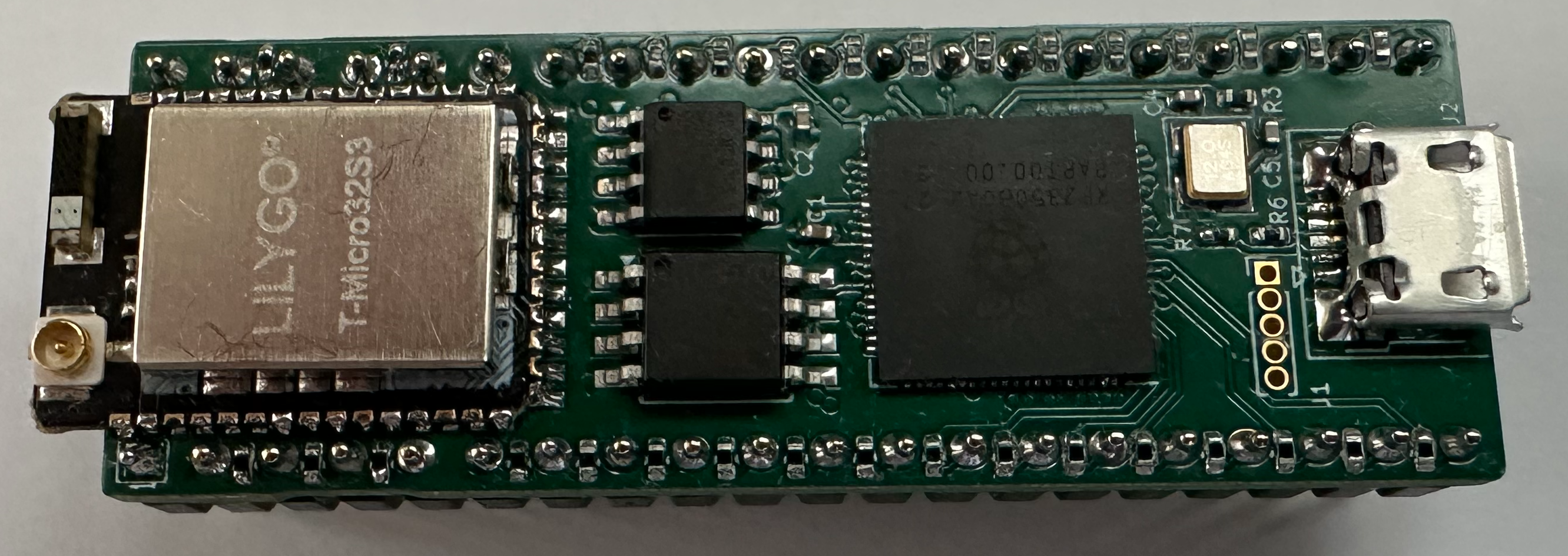
The pico6502 PCB (revision 2.2) is a compact 52mm × 19mm board that shares the same fundamental design as the picoZ80 but carries a 6502-specific bus interface rather than a Z80 interface. Four schematic sheets cover the RP2350B processor, the ESP32 co-processor, the 6502 bus interface, and the power supply. The USB hub present in the picoZ80 v2.5 is not fitted on the current pico6502 revision. All logic operates at 3.3V, with the bus interface designed for the 6502's 5V signal levels.
Key Components
- RP2350B (Cortex-M33 dual-core)
- primary processor at up to 300MHz. Core 1 runs the 6502 emulation hot loop; Core 0 handles file I/O, USB, and ESP32 relay. 512KB on-chip SRAM. - 16MB SPI Flash
- same layout as the picoZ80: bootloader, two 5MB application slots, two configuration slots, general config, and partition table. - 8MB PSRAM (SPI)
- 64 banks × 64KB of banked address space for the emulated 6502. Memory-block pointer arrays and I/O function-pointer arrays reside in PSRAM above the RAM/ROM area. - ESP32 co-processor
- WiFi, SD card, web server. Communicates with the RP2350 via 50MHz FSPI and 460.8kbaud UART. - SD card slot
- FAT32, managed by the ESP32. Storesconfig.json, ROM images, and disk images. - USB hub
- on-board USB hub for host connectivity and firmware update bridging. - 3.3V power supply
- buck converter from the 5V present on the 6502 DIP-40 VCC pin.
The pico6502 hardware is designed in KiCad. The current revision is v2.2. Schematic and PCB layout files are in the project repository under
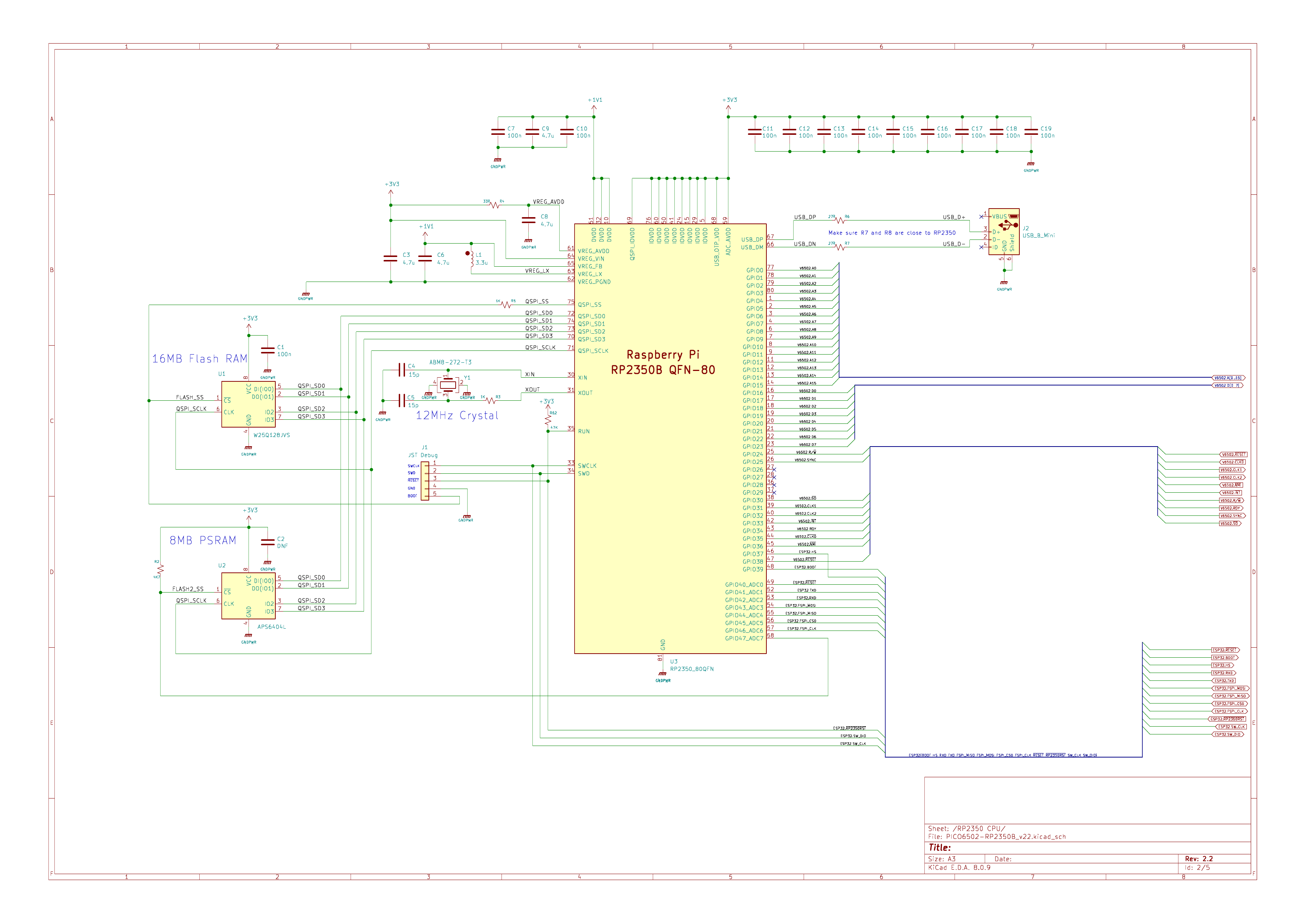
Sheet 1 — RP2350B Processor
kicad/PICO6502/.
The four schematic sheets are:
RP2350B QFN-80 GPIO assignments for the 6502 bus, 16MB Flash, 8MB PSRAM, and ESP32 communications. The 6502 bus requires A0–A15, D0–D7, PHI0/PHI1/PHI2, RNW, SYNC, IRQ, NMI, RDY, and RESET — consuming the majority of the RP2350B's 48 GPIO pins.
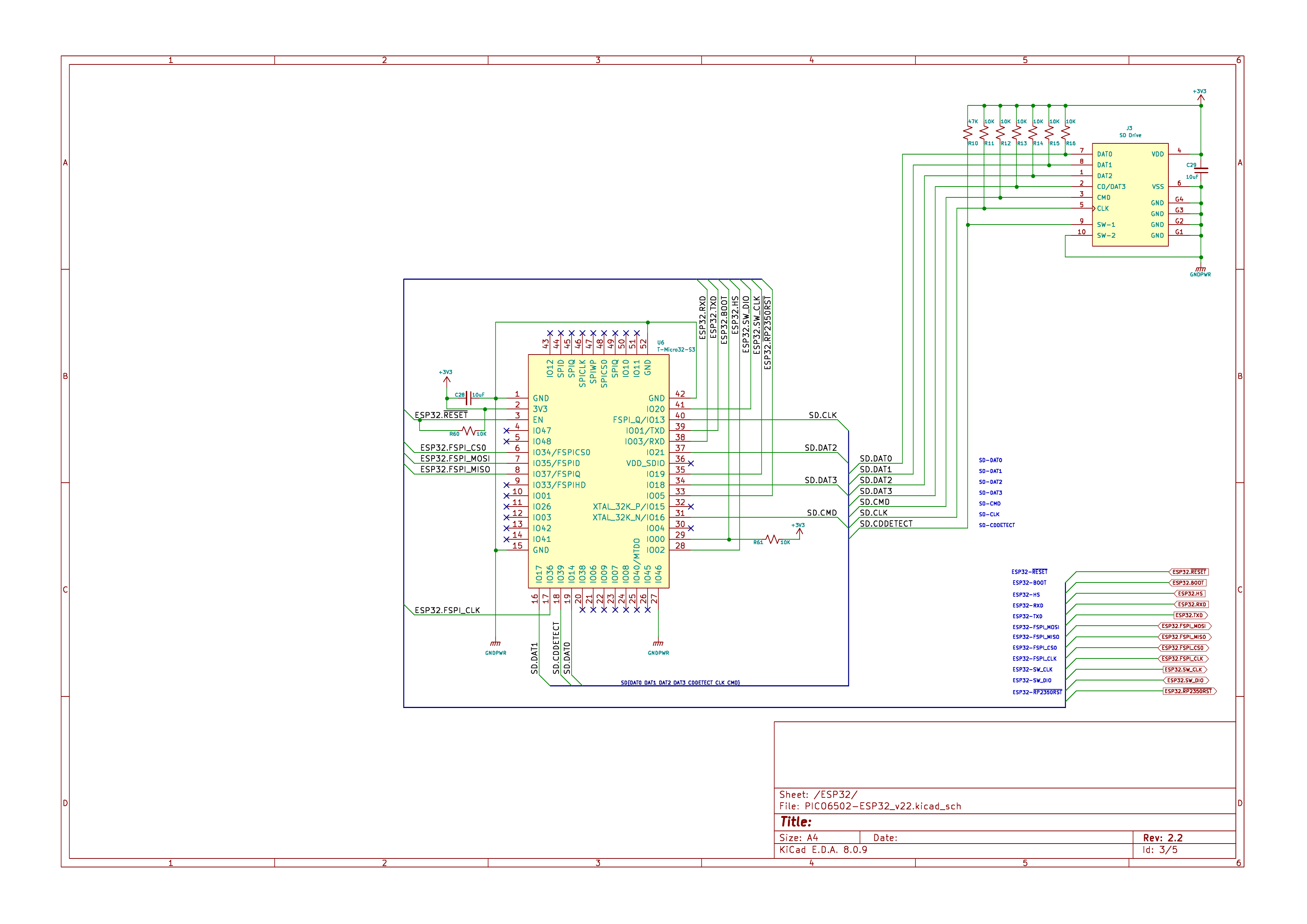
ESP32 module, SD card interface, antenna, and inter-processor communication (FSPI + UART). Identical in function to the picoZ80 design.
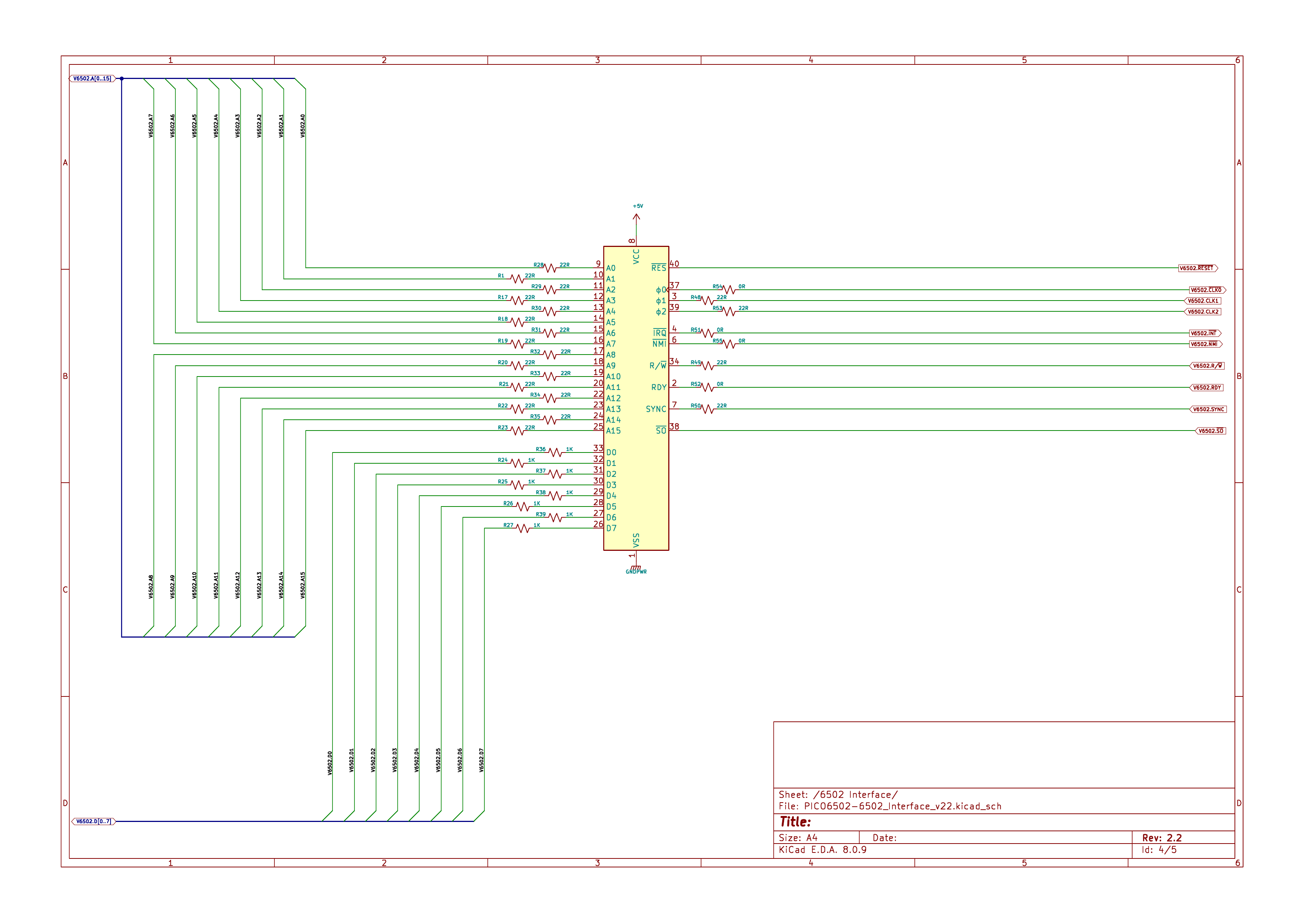
The DIP-40 socket connections and bus interface resistor network. Unlike the Z80, the 6502 has no separate I/O space — all peripherals are memory-mapped. All address, data, and control signals are routed through series resistors to RP2350 GPIO pins managed by the PIO state machines.
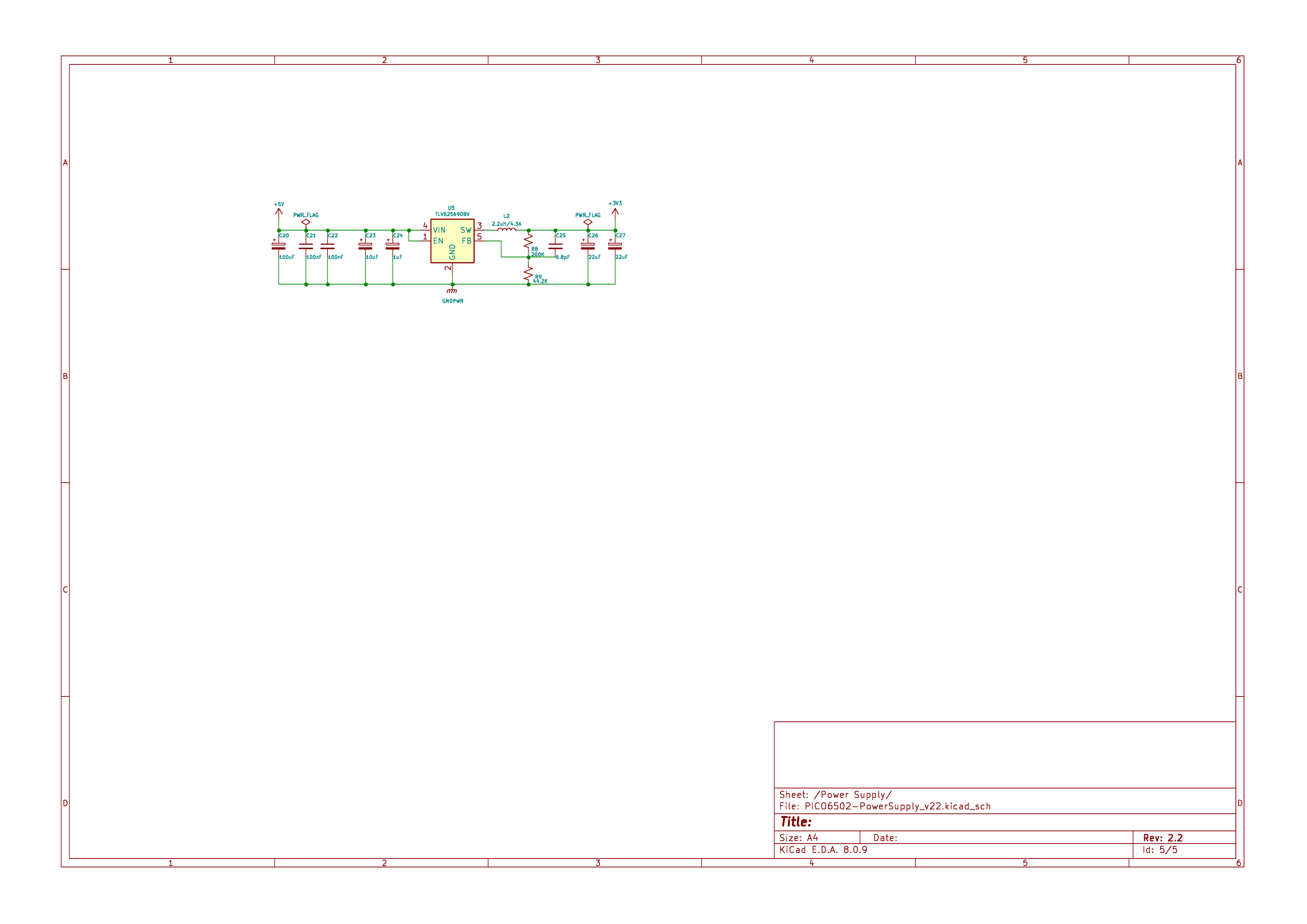
TLV62590BV 5V-to-3.3V synchronous buck converter with input/output filtering. Draws from the VCC pin of the 6502 DIP-40 socket.
KiCad source files:
kicad/PICO6502/PICO6502_Schematic.pdf (schematic PDF) and kicad/PICO6502/ (full KiCad project).
👀 Interactive BOM — pico6502 v2.2 (PCB component placement viewer)
")


Architecture
Dual-Core Design
The RP2350B core assignment mirrors the picoZ80:
Core 0 — USB bridge, firmware update coordination, file I/O relay to ESP32, ESP32 UART command dispatch, partition management.
Core 1 — The 6502 emulation hot loop. Services the PIO FIFOs to process 6502 bus transactions, resolves each address against the memory map, and dispatches to PSRAM, PHYSICAL pass-through, or FUNC virtual-device handlers. The inner loop runs from RP2350 SRAM for minimum latency.
Inter-core communication uses the same
PIO Bus Interface
queue_t message passing as the picoZ80, carrying messages for floppy/disk image changes, config reloads, file read/write, and firmware version queries.
The 6502 bus interface is implemented in
M6502.pio. The RP2350 provides three PIO blocks; the 6502 firmware uses all three:
- PIO 0 — Address and data bus (GPIO 0–23)
- runsm6502_addr(A0–A15, GPIO 0–15) andm6502_data(D0–D7, GPIO 16–23) simultaneously. Address words are pushed to the Core 1 FIFO; data is driven or sampled depending on RNW. - PIO 1 — Control signals and cycle execution (GPIO 16–47)
- runs the cycle sequencer (m6502_cycle), opcode fetch (m6502_fetch), memory read/write (m6502_read,m6502_write), IRQ detection (m6502_irq), NMI detection (m6502_nmi), and Set Overflow detection (m6502_so). - PIO 2 — Clock generation (GPIO 16–47)
- runsm6502_clock_6502, which generates the PHI1 and PHI2 two-phase non-overlapping clocks from an external PHI0 input, ensuring correct 6502 bus timing independent of Core 1 scheduling.
M6502.pio is:
| Program | Function |
|---|---|
m6502_clock_6502 |
Generates PHI1/PHI2 two-phase clocks from external PHI0. |
m6502_addr |
Outputs 16-bit address (A0–A15) and signals cycle start (IRQ 0). |
m6502_data |
Drives or samples D0–D7 (IRQ 1), with tri-state control. |
m6502_irq |
Detects IRQ assertion (IRQ flag 5). |
m6502_nmi |
Detects NMI assertion (IRQ flag 4). |
m6502_so |
Detects Set Overflow (SO) pin assertion (IRQ flag 6). |
m6502_cycle |
Top-level bus cycle sequencer; IRQ 7 signals exit from the execution loop. |
m6502_fetch |
Opcode-fetch bus cycle (PHI2 + RNW = read). |
m6502_read |
Memory read bus cycle. |
m6502_write |
Memory write bus cycle. |
State machines synchronise via PIO IRQ flags: IRQ 0 (address/cycle start), IRQ 1 (data phase), IRQ 4 (NMI), IRQ 5 (IRQ), IRQ 6 (SO), IRQ 7 (execution loop exit). The key difference from the Z80 interface is the 6502's two-phase clocking — PHI1 and PHI2 are non-overlapping; the address bus is valid on the PHI1 rising edge and data is presented or sampled before the PHI2 falling edge. Dedicating PIO 2 entirely to clock generation means the 6502 timing is always correct regardless of Core 1 activity.
Memory Model
The 6502 memory model is structurally identical to the Z80 model but without a separate I/O address space — because the 6502 has no IORQ equivalent, all peripheral registers appear in the 64KB memory map. The same three-tier architecture applies:
Tier 1 — RP2350 SRAM: 128-entry block-pointer array for O(1) dispatch per 512-byte block.
Tier 2 — PSRAM (8MB): 64 banks × 64KB RAM/ROM images and function-pointer arrays.
Tier 3 — Flash (16MB): firmware, ROM images, minified configuration JSON. Memory block types available for the 6502 memory map:
Tier 2 — PSRAM (8MB): 64 banks × 64KB RAM/ROM images and function-pointer arrays.
Tier 3 — Flash (16MB): firmware, ROM images, minified configuration JSON. Memory block types available for the 6502 memory map:
| Type | Description |
|---|---|
PHYSICAL |
Pass-through to real host hardware. |
PHYSICAL_VRAM |
Host video RAM with wait states. |
RAM |
Read/write — backed by PSRAM bank. |
ROM |
Read-only — backed by PSRAM bank. |
FUNC |
Virtual device — C handler called on every access. Used for all peripheral emulation, since the 6502 has no I/O space. |
PTR |
Per-byte redirect. |
Identical to the picoZ80 layout:
| Partition | Address Range | Size | Contents |
|---|---|---|---|
| Bootloader | 0x10000000–0x1001FFFF |
128KB | USB bridge, firmware update, partition selector |
| App Slot 1 | 0x10020000–0x1051FFFF |
5MB | Main 6502 firmware (partition 1) |
| App Slot 2 | 0x10520000–0x10A1FFFF |
5MB | Main 6502 firmware (partition 2) |
| App Config 1 | 0x10A20000–0x10C9FFFF |
2.5MB | ROM images + minified config JSON (slot 1) |
| App Config 2 | 0x10CA0000–0x10F1FFFF |
2.5MB | ROM images + minified config JSON (slot 2) |
| General Config | 0x10F20000–0x10FFEFFF |
892KB | Core settings, scratch space |
| Partition Table | 0x10FFF000–0x11000000 |
4KB | Active slot, checksums, metadata |
Build Instructions
The pico6502 uses the same build system and directory structure as the picoZ80. Please follow the picoZ80 build instructions for the full setup procedure — creating the root directory, setting
Clone the Project
PICO_PATH, running get_and_build_sdk.sh, and configuring the Docker alias for ESP-IDF. The differences specific to the pico6502 are noted below.
The pico6502 firmware does not require the Zeta Z80 emulator library. No projects/Z80 clone is needed.
mkdir -p <root>/projects
cd <root>/projects
git clone <tzpuPico-repo-url> tzpuPico
The same
build_tzpuPico.sh script is used. Ensure PICO_PATH is set correctly at the top of the script, then run from the root:
cd <root>

# Standard release build
./build_tzpuPico.sh

# Debug build
./build_tzpuPico.sh DEBUG

# Full build including ESP32 firmware via Docker
./build_tzpuPico.sh ALL
cd <root>/projects/tzpuPico/esp32
idf54 build
See the picoZ80 build instructions for the
Flashing
idf54 Docker alias definition.
The flashing procedure is identical to the picoZ80 — initial RP2350 flash via USB mass-storage, initial ESP32 flash via esptool, and subsequent updates via the OTA web pages. See the picoZ80 Flashing section for full details including the esptool command and board revision notes.
Configuration (JSON)
The pico6502 uses the same JSON configuration mechanism as the picoZ80. The top-level key is
"rp2350", with a "core" section for RP2350 operating parameters. The CPU-specific section uses the key "6502" (rather than "z80"), and since the 6502 has no separate I/O space, there is no "io" array — all peripheral mappings appear in the "memory" array as FUNC-type blocks.
{
  "esp32": {
    "core": {
      "device": "6502",
      "mode":   0
    },
    "wifi": {
      "override":  1,
      "wifimode":  "client",
      "ssid":      "MyNetwork",
      "password":  "MyPassword",
      "ip":        "192.168.1.192",
      "netmask":   "255.255.255.0",
      "gateway":   "192.168.1.1",
      "dhcp":      0,
      "webfs":     "webfs",
      "persist":   0
    }
  },
  "rp2350": {
    "core": {
      "cpufreq":   300000000,
      "psramfreq": 133000000,
      "voltage":   1.10
    },
    "6502": {
      "memory":  [ ... ],
      "drivers": [ ... ]
    }
  }
}
The
esp32.core
esp32 top-level object configures the ESP32 co-processor. It contains two sub-objects: core and wifi.
| Key | Type | Description |
|---|---|---|
device |
string | CPU device type — tells the ESP32 which processor personality to use. Valid values: "Z80" (picoZ80), "6502" (pico6502), "6512" (pico6512). |
mode |
integer | Default boot mode: 0 = client (station) mode, 1 = Access Point mode. Persisted in NVS. |
The
wifi object injects WiFi credentials and network settings from config.json, overriding whatever is stored in NVS. Set override to 0 to ignore this block and rely on previously persisted NVS settings.
| Key | Type | Description |
|---|---|---|
override |
0/1 | Master switch. 1 = apply all settings below; 0 = ignore this block and use persisted NVS settings. |
wifimode |
string | "ap" for Access Point mode; "client" for client/station mode. |
ssid |
string | WiFi network name to create (AP) or join (client). |
password |
string | WiFi passphrase. |
ip |
string | Fixed IP address (e.g. "192.168.1.192"). |
netmask |
string | Subnet mask (e.g. "255.255.255.0"). |
gateway |
string | Default gateway address. |
dhcp |
0/1 | Client mode only. 1 = DHCP; 0 = use fixed ip/netmask/gateway. |
webfs |
string | Override web filesystem root directory on SD card (default "webfs"). |
persist |
0/1 | 1 = write resolved settings back to NVS; 0 = apply for this session only. |
| Key | Type | Description |
|---|---|---|
cpufreq |
integer | RP2350 system clock frequency in Hz (e.g. 300000000 for 300 MHz). |
psramfreq |
integer | PSRAM SPI clock frequency in Hz (e.g. 133000000 for 133 MHz). |
voltage |
float | RP2350 core voltage (e.g. 1.10). |
Because the 6502 is a memory-mapped-I/O architecture, all peripherals appear in the
memory array. Use FUNC type for any address range that maps to a virtual device handler.
| Key | Type | Description |
|---|---|---|
enable |
0/1 | Whether this entry is active. |
addr |
hex string | Start address in the 6502 address space. |
size |
hex string | Region size. |
type |
string | PHYSICAL, PHYSICAL_VRAM, RAM, ROM, FUNC, PTR. |
bank |
integer | PSRAM bank number for RAM/ROM types. |
task |
string | Optional task identifier for FUNC-type blocks. |
file |
string | SD-card path to a ROM image to load at boot. |
"memory": [
  {
    "enable": 1,
    "addr":   "0xE000",
    "size":   "0x2000",
    "type":   "ROM",
    "bank":   0,
    "task":   "",
    "file":   "/ROM/host_bios.rom"
  },
  {
    "enable": 1,
    "addr":   "0x0000",
    "size":   "0xE000",
    "type":   "RAM",
    "bank":   0,
    "task":   "",
    "file":   ""
  },
  {
    "enable": 1,
    "addr":   "0xC000",
    "size":   "0x0010",
    "type":   "FUNC",
    "bank":   0,
    "task":   "via6522",
    "file":   ""
  }
]
The 6502 driver model is simpler than the Z80 model. Each driver entry loads one or more ROM images into PSRAM at startup. There are no address-remap or I/O-remap sub-tables; all memory layout is defined in the
memory array.
| Key | Type | Description |
|---|---|---|
enable |
0/1 | Whether this driver entry is active. |
name |
string | Descriptive name for this ROM load entry. |
rom |
array | ROM images to load into PSRAM at boot. |
rom[] entry:
| Key | Type | Description |
|---|---|---|
enable |
0/1 | Whether this ROM image is loaded. |
file |
string | SD-card path to the ROM binary. |
loadaddr |
array | Load address descriptors. |
loadaddr[] entry:
| Key | Type | Description |
|---|---|---|
enable |
0/1 | Whether this load address entry is active. |
position |
integer | Index within the file (for multi-ROM files). |
addr |
hex string | Destination address in the 6502 address space. |
bank |
integer | PSRAM bank to load into. |
size |
hex string | Number of bytes to load. |
"drivers": [
  {
    "enable": 1,
    "name":   "BIOS",
    "rom": [
      {
        "enable":   1,
        "file":     "/ROM/host_bios.rom",
        "loadaddr": [
          {
            "enable":   1,
            "position": 0,
            "addr":     "0xE000",
            "bank":     0,
            "size":     "0x2000"
          }
        ]
      }
    ]
  },
  {
    "enable": 1,
    "name":   "CharROM",
    "rom": [
      {
        "enable":   1,
        "file":     "/ROM/charrom.bin",
        "loadaddr": [
          {
            "enable":   1,
            "position": 0,
            "addr":     "0xB800",
            "bank":     0,
            "size":     "0x0800"
          }
        ]
      }
    ]
  }
]
A minimal configuration for a 6502 host with a 2KB zero-page/stack RAM area, 48KB general RAM, an 8KB BIOS ROM, and a VIA peripheral handler at
0xC000:
{
  "rp2350": {
    "core": {
      "cpufreq":   300000000,
      "psramfreq": 133000000,
      "voltage":   1.10
    },
    "6502": {
      "memory": [
        { "enable":1, "addr":"0x0000", "size":"0x0200",
          "type":"RAM", "bank":0, "task":"", "file":"" },
        { "enable":1, "addr":"0x0200", "size":"0xBE00",
          "type":"RAM", "bank":0, "task":"", "file":"" },
        { "enable":1, "addr":"0xC000", "size":"0x0010",
          "type":"FUNC", "bank":0, "task":"via6522", "file":"" },
        { "enable":1, "addr":"0xE000", "size":"0x2000",
          "type":"ROM", "bank":0, "task":"", "file":"/ROM/host_bios.rom" }
      ],
      "drivers": [
        {
          "enable":1, "name":"BIOS",
          "rom": [
            { "enable":1, "file":"/ROM/host_bios.rom",
              "loadaddr":[{ "enable":1, "position":0,
                            "addr":"0xE000", "bank":0, "size":"0x2000" }] }
          ]
        }
      ]
    }
  }
}
Web Interface
The pico6502 web interface is identical in structure to the picoZ80 interface — seven Bootstrap 4 pages served by the ESP32 at
http://<device-ip>/. Connect to the board's WiFi AP on first boot, then configure client mode via the WiFi Manager to join your network.
| Page | URL | Function |
|---|---|---|
| Dashboard | / |
Real-time system status: processor, device, firmware version, active partition. |
| Config Editor | /config.htm |
In-browser config.json editor with syntax highlighting and reload-without-reboot. |
| File Manager | /filemanager.htm |
SD-card file browser: upload, download, rename, delete. Transfer ROM images and disk images without removing the SD card. |
| Persona Selection | /personality.htm |
Select active machine persona per firmware partition. |
| ESP32 OTA | /ota-esp32.htm |
Upload ESP32 firmware over WiFi; upload versioned FilePack web filesystem archive to SD card. |
| RP2350 OTA | /ota-rp2350.htm |
Upload RP2350 firmware over WiFi; view and switch active partition. |
| WiFi Manager | /wifimanager.htm |
Configure WiFi SSID, password, and mode (AP or client). |
See the picoZ80 page for a detailed description of each web interface page — the pico6502 implementation is identical.
Reference Sites
The table below contains all the sites referenced in the design and programming of the pico6502.
| Site | Language | Description |
|---|---|---|
| RP2350 Datasheet | English | Official Raspberry Pi RP2350 technical reference and datasheet. |
| Pico SDK | English | Raspberry Pi Pico C/C++ SDK — build system and hardware abstraction used by the pico6502 firmware. |
| MOS 6502 Datasheet | English | Original MOS Technology 6502 MPU datasheet — bus timing, pin descriptions and electrical characteristics. |
| ESP-IDF | English | Espressif IoT Development Framework used for the ESP32 co-processor firmware. |
| 6502 Software Repository | English | Community 6502 software and ROM image repository. |
Manuals and Datasheets
The table below contains all the datasheets and manuals referenced in the design and programming of the pico6502.
| Datasheet | Language | Description |
|---|---|---|
| RP2350 | English | Raspberry Pi RP2350 microcontroller datasheet. |
| ESP32-S3 | English | Espressif ESP32-S3 SoC datasheet — WiFi/BT co-processor on the pico6502 board. |
| APS6404L PSRAM | English | 8MB SPI PSRAM datasheet — the main extended RAM used for memory banking. |
| W25Q128 Flash | English | Winbond 16MB SPI NOR Flash datasheet — stores firmware and ROM images. |
| TLV62590 | English | Texas Instruments 5V→3.3V synchronous buck converter powering the pico6502 from the 6502 DIP-40 VCC pin. |
| CH334F | English | CH334F 4-port USB 2.0 hub controller — provides USB hub functionality for firmware updates. |
Project Preview
The picoZ80 and pico6502 projects were first previewed on X (formerly Twitter):
https://x.com/engineerswork1/status/1953171627065188841
Demonstration Videos
Demonstration videos for the pico6502 will be added as the project matures. See the picoZ80 Demonstration Videos for examples of the shared platform in action.
Commercial Use Restriction
No commercial use permitted without express written permission.
The pico6502 hardware design (schematics, PCB layout, KiCad files), firmware, and all associated software are made available for personal, educational, and non-commercial use only. No part of this design — including but not limited to the PCB artwork, bill of materials, firmware binaries, source code, or documentation — may be used, reproduced, manufactured, sold, or incorporated into any commercial product or service without the express written permission of the author (Philip D. Smart).
To request a commercial licence or discuss permitted uses, please contact the author via the eaw.app website.
Credits
The pico6502 project builds on the work of several individuals and open-source projects. Their contributions are gratefully acknowledged.
- Manuel Sainz de Baranda y Goñi
Author of the Z80 C-language Z80 CPU emulator library (github.com/redcode/Z80), which is used by the companion picoZ80 project. The same high-accuracy emulation philosophy and shared firmware infrastructure informs the pico6502 design, and Manuel's work is gratefully acknowledged as part of the broader project family. - Raspberry Pi Ltd
Authors of the Pico SDK and RP2350 hardware. The PIO assembler, C SDK, CMake toolchain integration, and RP2350B silicon make the cycle-accurate 6502 bus interface possible. - Espressif Systems
Authors of the ESP-IDF framework and ESP32 hardware. The ESP32 co-processor, WiFi stack, OTA library, and NVS storage framework underpin the web management interface. - Philip Smart
Hardware design (KiCad schematics and PCB layout), RP2350 PIO firmware, ESP32 web application, JSON configuration system, and all project documentation. - Grok (xAI)
AI assistant that provided valuable help during PIO state machine debugging — particularly in diagnosing timing edge cases and cycle-accurate bus interaction issues in the RP2350 PIO programs. - Claude (Anthropic)
AI assistant contributing to this project across multiple areas: authoring and structuring the project documentation, analysing the FSPI/UART interface between the RP2350 and ESP32 and providing firmware improvement recommendations, and ongoing firmware development assistance.
Licenses
The pico6502 project is composed of several components, each covered by its own licence:
In short: the firmware and software you build from this project's source code are open-source under the GPL v3; the hardware designs are open-source under the CERN-OHL-P v2; third-party libraries retain their own licences as listed above.
| Component | Licence |
|---|---|
| pico6502 RP2350 firmware (PIO, C sources) | GNU General Public License v3 |
| pico6502 ESP32 firmware and web interface | GNU General Public License v3 |
| KiCad hardware design files (schematics, PCB) | CERN Open Hardware Licence v2 — Permissive (CERN-OHL-P v2) |
| Raspberry Pi Pico SDK | BSD 3-Clause |
| ESP-IDF framework | Apache License 2.0 |
| Bootstrap 4 (web interface) | MIT License |
The GNU General Public License v3
Copyright © 2024–2025 Philip Smart and contributors.
This program is free software: you can redistribute it and/or modify it under the terms of the GNU General Public License as published by the Free Software Foundation, either version 3 of the License, or (at your option) any later version.
This program is distributed in the hope that it will be useful, but WITHOUT ANY WARRANTY; without even the implied warranty of MERCHANTABILITY or FITNESS FOR A PARTICULAR PURPOSE. See the GNU General Public License for more details.
You should have received a copy of the GNU General Public License along with this program. If not, see https://www.gnu.org/licenses/.
The full licence text is also included in the repository as
LICENSE.