ZPU Evo(lution)
The ZPU is a 32bit Stack based microprocessor and was originally designed by Øyvind Harboe from Zylin AS and original documentation can be found on the Zylin/OpenCore website or Wikipedia. It is a microprocessor intended for FPGA embedded applications with minimal logic element and BRAM usage with the sacrifice of speed of execution.
Zylin produced two designs which it made open source, namely the Small and Medium ZPU versions. Additional designs were produced by external developers such as the Flex and ZPUino variations, each offering enhancements to the original design such as Wishbone interface, performance etc.
This document describes another design which I like to deem as the ZPU Evo(lution) model whose focus is on performance, connectivity and instruction expansion. This came about as I needed a CPU for an emulator of a vintage computer i am writing which would act as the IO processor to provide Menu, Peripheral and SD services.
An example of the performance of the ZPU Evo can be seen using CoreMark which returns a value of 22.2 @ 100MHz on Altera fabric using BRAM and for Dhrystone 13.2DMIPS. Comparisons can be made with the original ZPU designs in the gallery below paying attention to the CoreMark score which seems to be the defacto standard now. Connectivity can be seen via implementation of both System and Wishbone buses, allowing for connection of many opensource IP devices. Instruction expansion can be seen by the inclusion of a close coupled L1 cache where multiple instruction bytes are sourced and made available to the CPU which in turn can be used for optimization (ie. upto 5 IM instructions executed in 1 cycle) or for extended multi-byte instructions (ie. implementation of a LoaD Increment Repeat instruction). There is room for a lot more improvements such as stack cache, SDRAM to L2 burst mode, parallel instruction execution (ie. and + neqbranch) which are on my list.
The CPU
The ZPU Evo follows on from the ZPU Medium and Flex and areas of the code are similar, for example the instruction decoding. The design differs though due to caching and implementation of a Memory Transaction Processor where all Memory/IO operations (except for direct Instruction reads if dual-port instruction bus is enabled) are routed. The original CPU’s all handled their memory requirements in-situ or part of the state machine whereas the Evo submits a request to the MXP whenever a memory operation is required.
The following sections indicate some of the features and changes to original ZPU designs.
Bus structure
The ZPU has a linear address space with all memory and IO devices directly addressable within this space. Existing ZPU designs either provide a system bus or a wishbone bus whereas the Evo provides both. The ZPU Evo creates up to two distinct regions within the address space depending on configuration, to provide a system bus and a wishbone bus.
All models have the system bus instantiated which starts at cpu address 0 and expands up-to the limit imposed by the configurable maximum address bit (ie. 0x000000 - 0xFFFFFF for 24bit). A dedicated memory mapped IO region is set aside at the top of the address space (albeit it could quite easily be in any location) ie. 0xFF0000 - 0xFFFFFF.
If configured, a wishbone bus can be instantiated and this extends the maximum address bit by 1 (ie. 0x1000000 - 0x1FFFFFF for 24bit example). This in effect creates 2 identical regions, the lower being controlled via the system bus, the upper via the wishbone bus. As per the system bus, the upper area of the wishbone address space is reserved for IO devices.
A third bus can be configured, which is for instruction reads only. This bus typically shadows the system bus in memory region but is deemed to be connected to fast access memory for reading of instructions without the need for L2 Cache. This would typically be the 2nd port of a dual-port BRAM block with the 1st port connected to the system bus.
L1 Cache
In order to gain performance but more especially for instruction optimisations and extended instructions, an L1 cache is implemented using registers. Using registers consumes fabric space so should be very small but it allows random access in a single cycle which is needed for example if compacting a 32bit IM load (which can be 5 instructions) into a single cycle. Also for extended instructions, the first byte indicates an extended instruction and the following 1-5 bytes defines the instruction which is then executed in a single cycle.
L2 Cache
Internal BRAM (on-board Block RAM within the FPGA) doesn’t need an L2 Cache as it’s access time is 1-2 cycles. As BRAM is a limited resource it is assumed external RAM or SDRAM will be used which is much slower and this needs to be cached to increase throughput. The L2 Cache is used for this purpose, to read ahead a block of external RAM and feed the L1 Cache as needed. On analysis, the C programs generated by GCC are typically loops and calls within a local area (unless using large libraries), so implementing a simple direct mapping cache between external RAM and BRAM (used for the L2 Cache) indexed relative to the Program Counter is sufficient to keep the CPU from stalling most of the time.
Instruction Set
A feature of the ZPU is it’s use of a minimal fixed set of hardware implemented instructions and a soft set of additional instructions which are implemented in pseudo micro-code (ie. the fixed set of instructions). This is achieved by 32byte vectors in the region 0x0000 - 0x0400 and each soft instruction branches to the vector if it is not implemented in hardware. The benefit is reduced FPGA resources but the penalty is performance.
The ZPU Evo implements all instructions in hardware but this can be adjusted in the configuration to use soft instructions if required in order to conserve FPGA resources. This allows for a balance of resources versus performance. Ultimately though, if resources are tight then the use of the Small/Flex ZPU models may be a better choice.
In addition to the original instructions, a mechanism exists to extend the instruction set using multi-byte instructions of the format:-
Extend Instruction,<new insn[7:2]+ParamSize[1:0]>,[byte],[byte],[byte],[byte]
Where ParamSize =
- 00 - No parameter bytes,
- 01 - 8 bit parameter,
- 10 - 16 bit parameter,
- 11 - 32 bit parameter
Some extended instructions are under development (ie. LDIR) an exact opcode value and extended instruction set has not yet been fully defined. The GNU AS assembler will be updated with these instructions so they can be invoked within a C program and eventually if they have benefit to C will be migrated into the GCC compiler (ie. ADD32/DIV32/MULT32/LDIR/LDDR as from what I have seen, these will have a big impact on CoreMark/Dhrystone tests).
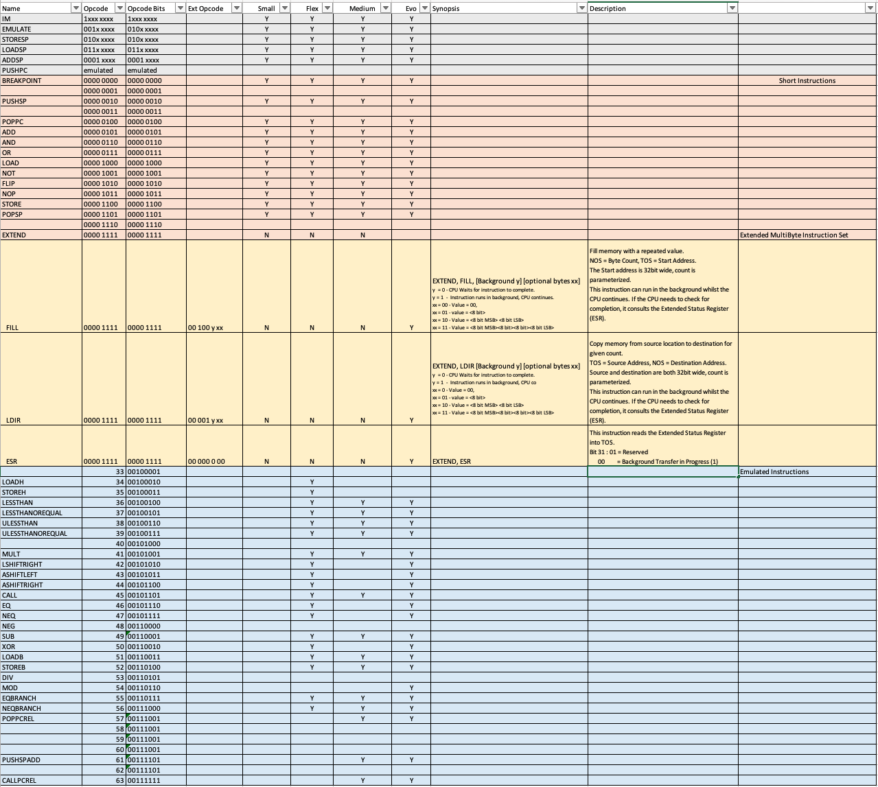
Implemented Instruction Set
| Name | Opcode | Description |
|---|---|---|
| ADD | 00000101 | Pops two values on stack adds them and pushes the result |
| ADDSP | 0001xxxx | Add value of memory location SP+xxxx*4 to value on top of stack. |
| AND | 00000110 | Pops two values off the stack and does a bitwise-and & pushes the result onto the stack |
| ASHIFTLEFT * | 00101011 | arithmetic(signed) shift left. long shift; long valX; shift = ((long) popIntStack()) & INTMASK; valX = ((long) popIntStack()) & INTMASK; int t = (int) (valX « (shift & 0x3f)); pushIntStack(t); |
| ASHIFTRIGHT * | 00101100 | arithmetic(signed) shift left. long shift; int valX; shift = ((long) popIntStack()) & INTMASK; valX = popIntStack(); int t = valX » (shift & 0x3f); pushIntStack(t); |
| BREAKPOINT | 00000000 | The debugger sets a memory location to this value to set a breakpoint. Once a JTAG-like debugger interface is added, it will be convenient to be able to distinguish between a breakpoint and an illegal(possibly emulated) instruction. |
| CALL * | 00101101 | call procedure. int address = pop(); push(pc + 1); setPc(address); |
| CALLPCREL * | 00111111 | call procedure pc relative int address = pop(); push(pc + 1); setPc(address+pc); |
| DIV * | 00110101 | Signed 32 bit integer divide. a = popIntStack(); b = popIntStack(); if (b == 0) { // undefined } pushIntStack(a / b); |
| EMULATE | 001xxxxx | Push PC to stack and set PC to 0x0+xxxxx*32. This is used to emulate opcodes. Emulated Opcodes are marked with a star (*) in this table. |
| EQ * | 00101110 | pushIntStack((popIntStack() == popIntStack()) ? 1 : 0); |
| EQBRANCH * | 00110111 | int compare; int target; target = popIntStack() + pc; compare = popIntStack(); if (compare == 0) { setPc(target); } else { setPc(pc + 1); } |
| ESR | E00000000 | Copy Extended Status Register to TOS. Bit 31 : 1 = reserved. Bit 0 = Background Transfer in Progress (1). |
| EXTEND | 00001111 | Extended instruction set. Byte following this instruction represents the new instruction. |
| FIADD32 * | 00111010 | Fixed point (Q15) addition. TOS and NOS are added and the result placed in TOS. |
| FIDIV32 * | 00111011 | Fixed point (Q15) division. TOS is the dividend, NOS is the divisor, result is placed in TOS. |
| FIMULT32 * | 00111100 | Fixed point (Q15) multiplication. TOS is multiplied by NOS and the result is placed in TOS. |
| FLIP | 00001010 | Reverses the bit order of the value on the stack, i.e. abc->cba, 100->001, 110->011, etc. The raison d’etre for this instruction is mainly to emulate other instructions. |
| IM | 1xxxxxxx | Pushes 7 bit sign extended integer and sets the a «instruction decode interrupt mask» flag(IDIM). If the IDIM flag is already set, this instruction shifts the value on the stack left by 7 bits and stores the 7 bit immediate value into the lower 7 bits. Unless an instruction is listed as treating the IDIM flag specially, it should be assumed to clear the IDIM flag. To push a 14 bit integer onto the stack, use two consecutive IM instructions. If multiple immediate integers are to be pushed onto the stack, they must be interleaved with another instruction, typically NOP. |
| LDIR | E00001yxx | LoaD Increment Repeat, copies <n> words of memory from source to destination. TOS = Source Address, NOS = Destination Address, xx = bytes to transfer where ‘01’ = 8 bit parameter, ‘10’ = 16 bit parameter, ‘11’ = 32 bit parameter. y = mode of operation, ‘0’ = CPU waits for completion, ‘1’ = Transfer operates in background. If a previous transfer is operating in the background, CPU waits for completion prior to executing instruction. Consult ESR for current status of background execution. |
| LESSTHAN * | 00100100 | Signed comparison a = popIntStack(); b = popIntStack(); pushIntStack((a < b) ? 1 : 0); |
| LESSTHANOREQUAL * | 00100101 | Signed comparison a = popIntStack(); b = popIntStack(); pushIntStack((a <= b) ? 1 : 0); |
| LOAD | 00001000 | Pops address stored on stack and loads the value of that address onto stack. Bit 0 and 1 of address are always treated as 0(i.e. ignored) by the HDL implementations and C code is guaranteed by the programming model never to use 32 bit LOAD on non-32 bit aligned addresses(i.e. if a program does this, then it has a bug). |
| LOADB * | 00110011 | 8 bit load instruction. Really only here for compatibility with C programming model. Also it has a big impact on DMIPS test. pushIntStack(cpuReadByte(popIntStack())&0xff); |
| LOADH * | 00100010 | 16 bit load instruction. Really only here for compatibility with C programming model. pushIntStack(cpuReadWord(popIntStack())); |
| LOADSP | 011xxxxx | Push value of memory location SP+xxxxx*4, where xxxxx is a positive integer, onto stack. |
| LSHIFTRIGHT * | 00101010 | unsigned shift right. long shift; long valX; int t; shift = ((long) popIntStack()) & INTMASK; valX = ((long) popIntStack()) & INTMASK; t = (int) (valX » (shift & 0x3f)); pushIntStack(t); |
| MOD * | 00110110 | Signed 32 bit integer modulo. a = popIntStack(); b = popIntStack(); if (b == 0) { // undefined } pushIntStack(a % b); |
| MULT * | 00101001 | Signed 32 bit multiply pushIntStack(popIntStack() * popIntStack()); |
| NEG * | 00110000 | pushIntStack(-popIntStack()); |
| NEQ * | 00101111 | pushIntStack((popIntStack() != popIntStack()) ? 1 : 0); |
| NEQBRANCH * | 00111000 | int compare; int target; target = popIntStack() + pc; compare = popIntStack(); if (compare != 0) { setPc(target); } else { setPc(pc + 1); } |
| NOP | 00001011 | No operation, clears IDIM flag as side effect, i.e. used between two consecutive IM instructions to push two values onto the stack. |
| NOT | 00001001 | Bitwise inverse of value on stack |
| OR | 00000111 | Pops two integers, does a bitwise or and pushes result |
| POPPC | 00000100 | Pops address off stack and sets PC |
| POPPCREL * | 00111001 | setPc(popIntStack()+getPc()); |
| POPSP | 00001101 | Pops value off top of stack and sets SP to that value. Used to allocate/deallocate space on stack for variables or when changing threads. |
| PUSHPC | emulated | Pushes program counter onto the stack. |
| PUSHSP | 00000010 | Pushes stack pointer. |
| PUSHSPADD * | 00111101 | a=sp; b=popIntStack()*4; pushIntStack(a+b); |
| STORESP | 010xxxxx | Pop value off stack and store it in the SP+xxxxx*4 memory location, where xxxxx is a positive integer. |
| STORE | 00001100 | Pops address, then value from stack and stores the value into the memory location of the address. Bit 0 and 1 of address are always treated as 0 |
| STOREB * | 00110100 | 8 bit store instruction. Really only here for compatibility with C programming model. Also it has a big impact on DMIPS test. addr = popIntStack(); val = popIntStack(); cpuWriteByte(addr, val); |
| STOREH * | 00100011 | 16 bit store instruction. Really only here for compatibility with C programming model. addr = popIntStack(); val = popIntStack(); cpuWriteWord(addr, val); |
| SUB * | 00110001 | int a=popIntStack(); int b=popIntStack(); pushIntStack(b-a); |
| ULESSTHAN * | 00100110 | Unsigned comparison long a; //long is here 64 bit signed integer long b; a = ((long) popIntStack()) & INTMASK; // INTMASK is unsigned 0x00000000ffffffff b = ((long) popIntStack()) & INTMASK; pushIntStack((a < b) ? 1 : 0); |
| ULESSTHANOREQUAL* | 00100111 | Unsigned comparison long a; //long is here 64 bit signed integer long b; a = ((long) popIntStack()) & INTMASK; // INTMASK is unsigned 0x00000000ffffffff b = ((long) popIntStack()) & INTMASK; pushIntStack((a <= b) ? 1 : 0); |
| XOR * | 00110010 | pushIntStack(popIntStack() ^ popIntStack()); |
E = Extended instruction, prefixed by EXTEND opcode.
* = Emulated instruction if not implemented in hardware.
Implemented Instructions Comparison Table
Hardware Variable Byte Write
In the original ZPU designs there was scope but not the implementation to allow the ZPU to perform byte/half-word/full-word writes. Either the CPU always had to perform 32bit Word aligned operations or it performed the operation in micro-code.
In the Evo, hardware was implemented (build time selectable) to allow Byte and Half-Word writes and also hardware Read-Update-Write operations. If the hardware Byte/Half-Word logic is not enabled then it falls back to the 32bit Word Read-Update-Write logic. Both methods have performance benefits, the latter taking 3 cycles longer.
Hardware Debug Serializer
In order to debug the CPU or just provide low level internal operating information, a cached UART debug module is implemented. Currently this is only for output but has the intention to be tied into the IOCP for in-situ debugging when Simulation/Signal-Tap is not available.
Embedded within the CPU RTL are selectable level triggered statements which issue snapshot information to the serialiser. The statements are expanded and then serialized and output to a connected terminal. A snapshot of the output information can be seen below (with manual comments):
| 000477 01ffec 00001ae4 00000000 70.17 04770484 046c047c 08f0046c 0b848015 17700500 05000500 05001188 11ef2004 Break Point - Illegal instruction PC Stack TOS NOS Insn Signals Signals Signals Signals L1 Insn Q L1 Insn Q L1 Insn Q L1 Insn Q 000478 01ffe8 00001ae4 00001ae4 00.05 04780484 046c0478 08f0046c 0b888094 05000500 05000500 118811ef 20041188 L1 Cache Dump 000478 (480)-> 11 e2 2a 51 11 a0 11 8f <-(483) (004)->11 ed 20 04 05 00 05 00 05 00 05 00 05 00 05 00 20 (46c)->04 11 b5 11 e4 17 70 <-(46f) (004)-> 11 ed 20 04 05 00 05 00 05 00 05 00 05 00 05 00 20 (46c)->04 11 b5 11 e4 17 70 11 b6 11 c4 2d 27 11 8b <-(473) 05 00 05 00 05 00 05 00 (46c)->20 04 11 b5 11 e4 17 70 11 b6 11 c4 2d 27 11 8b 1c 38 11 80 17 71 17 70 -<(477) (46c)->20 04 11 b5 11 e4 17 70 11 b6 11 c4 2d 27 11 8b 1c 38 11 80 17 71 17 70 -<(477) 05 00 05 00 05 00 05 00 (470)->11 b6 11 c4 2d 27 11 8b 1c 38 11 80 17 71 17 70 <-(477) -> 05 00 05 00 05 00 05 00 (47c)->11 88 11 ef 20 04 11 88 <-(47f) (474)->1c 38 11 80 17 71 17 70 05 00 05 00 05 00 05 00 11 88 11 ef 20 04 11 88 11 e2 2a 51 11 a0 11 8f 05 00 05 00 05 00 05 00 11 88 11 ef 20 04 11 88 11 e2 2a 51 11 a0 11 8f 11 ed 20 04 05 00 05 00 11 88 11 ef 20 04 11 88 11 e2 2a 51 11 a0 11 8f 11 ed 20 04 05 00 05 00 05 00 05 00 05 00 05 00 L2 Cache Dump 000000 88 08 8c 08 ed 04 00 00 00 00 00 00 00 00 00 00 00 00 00 00 00 00 00 00 00 00 00 00 00 00 00 00 000020 88 08 8c 08 90 08 0b 0b 0b 88 80 08 2d 90 0c 8c 0c 88 0c 04 00 00 00 00 00 00 00 00 00 00 00 00 000040 71 fd 06 08 72 83 06 09 81 05 82 05 83 2b 2a 83 ff ff 06 52 04 00 00 00 00 00 00 00 00 00 00 00 |
All critical information such as current instruction being executed (or not if stalled), Signals/Flags, L1/L2 Cache contents and Memory contents can be output.
Timing Constraints
This is a work in progress, I am slowly updating the design and/or adding constraints such that timing is fully met. Currently there is negative slack at 100MHz albeit the design fully works, this will in the future be corrected so timing as analyzed by TimeQuest will be met.
System On a Chip
In order to provide a working framework in which the ZPU Evo could be used, a System On a Chip wrapper was created which allows for the instantiation of various devices (ie. UART/SD card).
As part of the development, the ZPU Small/Medium/Flex models were incorporated into the framework allowing the choice of CPU when fabric space is at a premium or comparing CPU’s, albeit features such as Wishbone are not available on the original ZPU models. I didn’t include the ZPUino as this design already has a very good eco system or the ZY2000.
The SoC currently implements (in the build tree):
| Component | Option | Comment |
|---|---|---|
| CPU | Yes | ZPU Small, Medium, Flex, Evo or Evo Minimal. |
| Wishbone Bus | Yes | 32 bit Wishbone bus. |
| (SB) BRAM | Yes | Implement a configurable block of BRAM as the boot loader and stack. |
| Instruction Bus BRAM | Yes | Enable a separate bus (or Dual-Port) to the boot code implemented in BRAM. This is generally a dual-port BRAM shared with the Sysbus BRAM but can be independent. |
| (SB) RAM | Yes | Implement a block of BRAM as RAM, seperate from the BRAM used for the boot loader/stack. |
| (WB) SDRAM | Yes | Implement an SDRAM controller over the Wishbone bus. |
| (WB) RAM | Yes | Implement a block of BRAM as RAM over the Wishbone bus. |
| (WB) I2C | Yes | Implements an I2C Controller over the Wishbone bus. |
| (SB) Timer 0 | No | Implements a hardware 12bit Second, 18bit milliSec and 24bit uSec down counter with interrupt, a 32bit milliSec up counter with interrupt and a YMD HMS Real Time Clock. The down counters are ideal for scheduling. |
| (SB) Timer 1 | Yes | A selectable number of pre-scaled 32bit down counters. |
| (SB) UART 0 | No | A cached UART used for monitor output and command input/program load. |
| (SB) UART 1 | No | A cached UART used for software (C program)/hardware (ZPU debug serializer) output. |
| (SB) Interrupt Controller | Yes | A prioritized configurable (# of inputs) interrupt controller. |
| (SB) PS2 | Yes | A PS2 Keyboard and Mouse controller. |
| (SB) SPI | Yes | A configurable number of Serial Peripheral Interface controllers. |
| (SB) SD | Yes | A configurable number of hardware based SPI SD controllers. |
| (SB) SOCCFG | Yes | A set of registers to indicate configuration of the ZPU and SoC to the controlling program. |
Within the SoC configuration, items such as starting Stack Address, Reset Vector, IO Start/End (SB) and (WB) can be specified. With the addition of the wishbone bus, it is very easy to add further opencore IP devices, for the system bus some work may be needed as the opencore IP devices use differing signals.
SDRAM
Software
The software provided includes:
- A bootloader, I/O Control Program (IOCP). This is more than a bootloader, in its basic form it can bootstrap an application from an SD card or it can include command line monitor tools and a serial upload function.
- An application, ZPUTA (ZPU Test Application). This is a test suite and can be organised as a single application or split into a Disk Operating System where all functionality is stored on the SD card. ZPUTA can be bootstrapped by IOCP or standalone as the only program in the ROM/BRAM.
- A disk operating system, zOS (ZPU Operating System). A version of ZPUTA but aimed at production code where all functionality resides as disk applications.
- Library functions in C to aid in building applications, including 3rd party libs ie. FatFS from El. Chan
21/04/2020: Software for the ZPU has now been merged with the tranZPUter and is kept and maintained in the zSoft repository.
Configuration
This section shows how to configure the ZPU and the SoC, either to use the ZPU seperately or as part of the included SoC.
Configure the CPU
The CPU is configurable using the configuration file ‘cpu/zpu_pkg.vhd’. It generally specifies the size of the address bus and what hardware features should be enabled. The following table outlines the configurable options.
| Configuration Variable | Model | Values | Description | |
|---|---|---|---|---|
| EVO_USE_INSN_BUS | Evo | true/false | Use a seperate instruction bus to connect to the BRAM memory. All other Memory and I/O operations will go over the normal bus. This option is primarily used with Dual Port BRAM, one side connected to the Instruction Bus the other side to the standard bus and will give a significant performance boost when the executed code is in this memory. | |
| EVO_USE_HW_BYTE_WRITE | Evo | true/false | This option implements hardware writing of bytes, reads are always 32bit and aligned. | |
| EVO_USE_HW_WORD_WRITE | Evo | true/false | This option implements hardware writing of 16bit words, reads are always 32bit and aligned. | |
| EVO_USE_WB_BUS | Evo | true/false | Implement the wishbone interface in addition to the system bus. | |
| DEBUG_CPU | All | true/false | Enable CPU debugging output. This generally consists of core data being serialised and output via the UART1 TX. There are pre-defined blocks of debug data (debug level) for output but it is easy to add in another if your targetting a specific CPU area/instruction. | |
| DEBUG_LEVEL | All | 0 to 5 | Level of debugging output. 0 = Basic, such as Breakpoint, 1 =+ Executing Instructions, 2 =+ L1 Cache contents, 3 =+ L2 Cache contents, 4 =+ Memory contents, 5=+ Everything else. | |
| DEBUG_MAX_TX_FIFO_BITS | All | 2 .. ~16 | Size of UART TX Fifo for debug output. One point to note, if too much data is output and the output Baud rate too low, the CPU will wait so cache size is irrelevant. Cache is only useful if outputting small amounts of data (ie. a targetted instruction) where the cache never becomes full and the CPU doesnt need to wait. | |
| DEBUG_MAX_FIFO_BITS | All | 2 .. ~16 | Size of debug output data records fifo. Each request to output data via the serialiser is made via debug records which consume memory, the more records available the less chance of the CPU stalling. | |
| DEBUG_TX_BAUD_RATE | All | Any Baud integer value | This option sets the output Baud rate of the debug serializer transmitter, ie. 115200 | |
| maxAddrBit | All | <16..31n> + WB_ACTIVE | This option sets the width of the address bus. WB_ACTIVE adds 1 to the width of the bus if the WishBone bus is enabled as the wishbone bus operates in the top half of the addressable memory area. |
- The ZPU Evo has a number of options to enable/disable hardware instructions and cache. When instantiating a ZPU Evo CPU, the following options can be set to the desired configuration:
| Configuration Variable | Values | Description | |
|---|---|---|---|
| IMPL_OPTIMIZE_IM | true/false | If the instruction cache is enabled, optimise Im instructions to gain speed. | |
| IMPL_ASHIFTLEFT | true/false | Arithmetic Shift Left (uses same logic so normally combined with ASHIFTRIGHT and LSHIFTRIGHT). | |
| IMPL_ASHIFTRIGHT | true/false | Arithmetic Shift Right. | |
| IMPL_CALL | true/false | Call to direct address. | |
| IMPL_CALLPCREL | true/false | Call to indirect address (add offset to program counter). | |
| IMPL_DIV | true/false | 32bit signed division. | |
| IMPL_EQ | true/false | Equality test. | |
| IMPL_EXTENDED_INSN | true/false | Extended multibyte instruction set. | |
| IMPL_FIADD32 | true/false | Fixed point Q17.15 addition. | |
| IMPL_FIDIV32 | true/false | Fixed point Q17.15 division. | |
| IMPL_FIMULT32 | true/false | Fixed point Q17.15 multiplication. | |
| IMPL_LOADB | true/false | Load single byte from memory. | |
| IMPL_LOADH | true/false | Load half word (16bit) from memory. | |
| IMPL_LSHIFTRIGHT | true/false | Logical shift right. | |
| IMPL_MOD | true/false | 32bit modulo (remainder after division). | |
| IMPL_MULT | true/false | 32bit signed multiplication. | |
| IMPL_NEG | true/false | Negate value in TOS. | |
| IMPL_NEQ | true/false | Not equal test. | |
| IMPL_POPPCREL | true/false | Pop a value into the Program Counter from a location relative to the Stack Pointer. | |
| IMPL_PUSHSPADD | true/false | Add a value to the Stack pointer and push it onto the stack. | |
| IMPL_STOREB | true/false | Store/Write a single byte to memory/IO. | |
| IMPL_STOREH | true/false | Store/Write a half word (16bit) to memory/IO. | |
| IMPL_SUB | true/false | 32bit signed subtract. | |
| IMPL_XOR | true/false | Exclusive or of value in TOS. | |
| RESET_ADDR_CPU | <n> | Initial address to start execution from after reset. This is normally set as the start of the firmware in ROM/BRAM. | |
| START_ADDR_MEM | <n> | Start location of program memory. This is normally set as the start of the firmware in ROM/BRAM. | |
| STACK_ADDR | <n> | Stack start address. This is normally set as the top of the RAM/BRAM less 2 words. | |
| CLK_FREQ | <n> | This is the cpu clock frequency in Hertz. It is used primarily for the debug logic and output UART baud rate generator. |
Configure the SoC
The System on a Chip is configurable using the configuration file ‘zpu_soc_pkg.vhd’. The following table outlines the options which can be configured to adapt the SoC to a specific application.
- The following options allow you to choose which CPU to instantiate depending on your requirements. Warning, only one can be enbled!
| Configuration Variable | Values | Description | |
|---|---|---|---|
| ZPU_SMALL | <0 or 1> | Select the SMALL CPU to be used in the SoC. NB. Wishbone interface not available for this CPU. | |
| ZPU_MEDIUM | <0 or 1> | Select the MEDIUM CPU to be used in the SoC. NB. Wishbone interface not available for this CPU. | |
| ZPU_FLEX | <0 or 1> | Select the FLEX CPU to be used in the SoC. NB. Wishbone interface not available for this CPU. | |
| ZPU_EVO | <0 or 1> | Select the EVOLUTION CPU to be used in the SoC. | |
| ZPU_EVO_MINIMAL | <0 or 1> | Select the Minimalist EVOLUTION CPU, which is the EVO CPU with all configurable options disabled using less fabric. |
- The following options set the frequencies for the various boards. Normally these dont need changing, add additional constants if using a different board to those defined and add in your
_Topleavel.vhd file. NB. This option only changes logic dependent on frequency, it doesnt change the PLL which needs to be done seperately in HDL.
| Configuration Variable | Values | Description | |
|---|---|---|---|
| SYSCLK_E115_FREQ | <Freq in Hz> | Set the frequency for the E115 FPGA Board. | |
| SYSCLK_QMV_FREQ | <Freq in Hz> | Set the frequency for the QMTECH Cyclone V FPGA Board. | |
| SYSCLK_DE0_FREQ | <Freq in Hz> | Set the frequency for the DE0-Nano FPGA Board. | |
| SYSCLK_DE10_FREQ | <Freq in Hz> | Set the frequency for the DE10-Nano FPGA Board. | |
| SYSCLK_CYC1000_FREQ | <Freq in Hz> | Set the frequency for the Trenz CYC1000 FPGA Board. | |
| SYSTEM_FREQUENCY | 100000000 | Default system clock frequency if not overriden by the above values in the top level. |
- Set the ID’s for the various ZPU models. The format is 2 bytes, MSB=<Model>, LSB=<Revision>. This is only necessary if your making a different version and you need to detect in your software.
| Configuration Variable | Values | Description | |
|---|---|---|---|
| ZPU_ID_SMALL | 16#0101# | Set ID for the ZPU Small in this package. | |
| ZPU_ID_MEDIUM | 16#0201# | Set ID for the ZPU Medium in this package. | |
| ZPU_ID_FLEX | 16#0301# | Set ID for the ZPU Flex in this package. | |
| ZPU_ID_EVO | 16#0401# | Set ID for the ZPU Evo in this package. | |
| ZPU_ID_EVO_MINIMAL | 16#0501# | Set ID for the ZPU Evo Minimal in this package. |
- EVO CPU cache specific configuration.
| Configuration Variable | Values | Description | |
|---|---|---|---|
| MAX_EVO_L1CACHE_BITS | <3..n>, ie.5 | Evo. Set the maximum size in instructions of the Level 0 instruction cache governed by the number of bits, ie. 8 = 256 instruction cache. NB. This option uses fabric registers so use sparingly. | |
| MAX_EVO_L2CACHE_BITS | <8..n>, ie.14 | Evo. Set the maximum bit size in bytes of the Level 2 instruction cache governed by the number of bits, ie. 8 = 256 byte cache. This option uses BRAM. | |
| MAX_EVO_MXCACHE_BITS | <3..n>, ie.3 | Evo. Set the maximum size of the memory transaction cache governed by the number of bits. This option changes the depth of the requests made by the CPU to the Memory Transaction Processor. No checks are made if the cache becomes full as it is finite and can be determined in the design how many slots will be used. | |
| MAX_EVO_MIN_L1CACHE_BITS | <3..n>, ie.3 | Minimal Evo. Set the maximum size in instructions of the Level 0 instruction cache governed by the number of bits, ie. 8 = 256 instruction cache. NB. This option uses fabric registers so use sparingly. | |
| MAX_EVO_MIN_L2CACHE_BITS | <8..n>, ie.12 | Minimal Evo. Set the maximum bit size in bytes of the Level 2 instruction cache governed by the number of bits, ie. 8 = 256 byte cache. This option uses BRAM. | |
| MAX_EVO_MIN_MXCACHE_BITS | <3..n>, ie.3 | Minimal Evo. Set the maximum size of the memory transaction cache governed by the number of bits. |
- Settings for various IO devices.
| Configuration Variable | Values | Description | |
|---|---|---|---|
| MAX_RX_FIFO_BITS | <4..n>, ie.4 | Size of the UART RX Fifo. | |
| MAX_TX_FIFO_BITS | <4..n>, ie.10 | Size of UART TX Fifo. | |
| MAX_UART_DIVISOR_BITS | <1..n>, ie.16 | Maximum number of bits for the UART clock rate generator divisor. | |
| INTR_MAX | <1..n>, ie.16 | Maximum number of interrupt inputs. |
- SoC specific options.
| Configuration Variable | Values | Description | |
|---|---|---|---|
| SOC_IMPL_TIMER1 | true/false | Implement Timer 1, an array of prescaled downcounter with enable. | |
| SOC_TIMER1_COUNTERS | <0..n>, ie.0 | Number of downcounters in Timer 1. Value is a 2^ array of counters, so 0 = 1 counter. | |
| SOC_IMPL_SD | true/false | Implement SD Card interface. | |
| SOC_SD_DEVICES | <0..n> | Number of SD card channels implemented. | |
| SOC_IMPL_INTRCTL | true/false | Implement the prioritised interrupt controller. | |
| SOC_IMPL_TCPU | true/false | Implement the TCPU controller for controlling the Z80 Bus. | |
| SOC_IMPL_SOCCFG | true/false | Implement the SoC Configuration information registers. |
- Main Boot BRAM on sysbus, contains startup firmware.
| Configuration Variable | Values | Description | |
|---|---|---|---|
| SOC_IMPL_BRAM | true/false | Implement BRAM for the BIOS and initial Stack. | |
| SOC_IMPL_INSN_BRAM | true/false | Implement dedicated instruction BRAM for the EVO CPU. Any addr access beyond the BRAM size goes to normal memory. | |
| SOC_MAX_ADDR_BRAM_BIT | <n>, ie.15 | Max address bit of the System BRAM ROM/Stack in bytes, ie. 15 = 32KB or 8K 32bit words. NB. For non evo CPUS you must adjust the maxMemBit parameter in zpu_pkg.vhd to be the same. | |
| SOC_ADDR_BRAM_START | <n>, ie.0 | Start address of BRAM. |
- Secondary block of sysbus RAM, typically implemented in BRAM.
| Configuration Variable | Values | Description | |
|---|---|---|---|
| SOC_IMPL_RAM | true/false | Implement RAM using BRAM, typically for Application programs seperate to BIOS. | |
| SOC_MAX_ADDR_RAM_BIT | <n>, ie.14 | Max address bit of the System RAM. | |
| SOC_ADDR_RAM_START | <n>, ie.32768 | Start address of RAM. |
- SDRAM on sysbus
| Configuration Variable | Values | Description | |
|---|---|---|---|
| SOC_IMPL_SDRAM | true/false | Implement Dynamic RAM and controller. | |
| SOC_MAX_ADDR_SDRAM_BIT | <n>, ie.22 | Max address bit of the System RAM. | |
| SOC_ADDR_SDRAM_START | <n>, ie.65536 | Start address of RAM. |
- SDRAM on Wishbone bus.
| Configuration Variable | Values | Description | |
|---|---|---|---|
| SOC_IMPL_WB_SDRAM | true/false | Implement SDRAM over wishbone interface. | |
| SOC_MAX_ADDR_WB_SDRAM_BIT | <n>, ie.22 | Max address bit of the System RAM. | |
| SOC_ADDR_WB_SDRAM_START | <n>, ie.16777216 | Start address of RAM. |
- Instruction BRAM on sysbus, typically as a 2nd port on the main Boot BRAM (ie. dualport).
| Configuration Variable | Values | Description | |
|---|---|---|---|
| SOC_ADDR_INSN_BRAM_START | <n>, ie.0 | If the instruction bus is enabled this varialble indicates the address at which the BRAM starts on the instruction bus. |
- Options for the CPU initialisation.
| Configuration Variable | Values | Description | ||
|---|---|---|---|---|
| SOC_RESET_ADDR_CPU | <n> | Initial address to start execution from after reset. This is normally set as the start of BRAM, ie. SOC_ADDR_BRAM_START | ||
| SOC_START_ADDR_MEM | <n> | Start location of program memory (BRAM/ROM/RAM). This is normally set as the start of BRAM, ie. SOC_ADDR_BRAM_START | ||
| SOC_STACK_ADDR | <n> | Stack start address (BRAM/RAM). This is normally set as the top of the BRAM less 2 words, ie. SOC_ADDR_BRAM_END - 8 | ||
| SOC_ADDR_IO_START | <n> | Start address of the Evo system bus IO region. This is normally via the forumula: ‘2^(maxAddrBit-WB_ACTIVE)) - (2^maxIOBit)’ which sets the address space based on the address bus width and wether the wishbone bus is implemented. | ||
| SOC_ADDR_IO_END | <n> | End address of the Evo system bus IO region. This is normally via the formula: (2^(maxAddrBit-WB_ACTIVE)) - 1 | ||
| SOC_WB_IO_START | <n>, ie. 32505856 | Start address of the Wishbone bus IO range. | ||
| SOC_WB_IO_END | <n>, ie. 33554431 | End address of the Wishbone bus IO range. |
- The ZPU Evo can be configured ia the SoC configuration to enable/disable desired options. Two sets of values exist, one with _EVO_ for the normal ZPU Evo instantiation, the other with _EVOM_ for the ZPU Minimal Evo instantiation.
- The configurable options are as follows:
| Configuration Variable | Values | Description | |
|---|---|---|---|
| IMPL_EVO_OPTIMIZE_IM | true/false | If the instruction cache is enabled, optimise Im instructions to gain speed. |
- Evo CPU instructions to be implemented in hardware:
| Configuration Variable | Values | Description | |
|---|---|---|---|
| IMPL_EVO_ASHIFTLEFT | true/false | Arithmetic Shift Left (uses same logic so normally combined with ASHIFTRIGHT and LSHIFTRIGHT). | |
| IMPL_EVO_ASHIFTRIGHT | true/false | Arithmetic Shift Right. | |
| IMPL_EVO_CALL | true/false | Call to direct address. | |
| IMPL_EVO_CALLPCREL | true/false | Call to indirect address (add offset to program counter). | |
| IMPL_EVO_DIV | true/false | 32bit signed division. | |
| IMPL_EVO_EQ | true/false | Equality test. | |
| IMPL_EVO_EXTENDED_INSN | true/false | Extended multibyte instruction set. | |
| IMPL_EVO_FIADD32 | true/false | Fixed point Q17.15 addition. | |
| IMPL_EVO_FIDIV32 | true/false | Fixed point Q17.15 division. | |
| IMPL_EVO_FIMULT32 | true/false | Fixed point Q17.15 multiplication. | |
| IMPL_EVO_LOADB | true/false | Load single byte from memory. | |
| IMPL_EVO_LOADH | true/false | Load half word (16bit) from memory. | |
| IMPL_EVO_LSHIFTRIGHT | true/false | Logical shift right. | |
| IMPL_EVO_MOD | true/false | 32bit modulo (remainder after division). | |
| IMPL_EVO_MULT | true/false | 32bit signed multiplication. | |
| IMPL_EVO_NEG | true/false | Negate value in TOS. | |
| IMPL_EVO_NEQ | true/false | Not equal test. | |
| IMPL_EVO_POPPCREL | true/false | Pop a value into the Program Counter from a location relative to the Stack Pointer. | |
| IMPL_EVO_PUSHSPADD | true/false | Add a value to the Stack pointer and push it onto the stack. | |
| IMPL_EVO_STOREB | true/false | Store/Write a single byte to memory/IO. | |
| IMPL_EVO_STOREH | true/false | Store/Write a half word (16bit) to memory/IO. | |
| IMPL_EVO_SUB | true/false | 32bit signed subtract. | |
| IMPL_EVO_XOR | true/false | Exclusive or of value in TOS. |
Build
This section shows how to make a basic build and assumes the target development board is the QMTECH Cyclone V board. There are many configuration options but these will be covered seperately.
Software build
Jenkins can be used to automate the build but for simple get up and go compilation use the build.sh and hierarchical Makefile system following the basic instructions here.
- Download and install the ZPU GCC ToolChain. Install into /opt or similar common area.
- Setup the environment variable path.
export PATH=$PATH:/opt/zpu/bin - Clone the ZPU Evo repository
- Edit the <zpu evo dir>/software/zputa/zputa.h file and select which functions you want building into the zputa core image (by default, all functions are built as applets but these will be ignored if they are built into the zputa core image). You select a function by setting the BUILTIN_
to '1', set to '0' if you dont want it built in. - Decide which memory map you want and wether ZPUTA will be an application or bootloader (for your own applications, it is they same kind of choice), see build.sh in the table below for options. Once decided, issue the build command.
cd <zpu evo dir>/software # For this build we have chosen a Tiny IOCP Bootloader, building ZPUTA as an # application with a Tiny IOCP bootloader, the ZPUTA Base Address is 0x1000 # and the address where Applets are loaded and executed is at 0xC000 ./build.sh -I 3 -O zputa -o 2 -B 0x1000 -A 0xC000 # The build command automatically creates the VHDL BRAM images with the IOCP # Bootloader installed, thus you will need to build the ZPU Evo SOF bit stream # and upload it to the FPGA in order for the new Bootloader to be active. - Place an SD Card into your system and format it for FAT32 format then copy the files onto it.
 cd build/SD
 cp -r * <abs path to SD card, ie. /media/psmart/ZPU>
 # eject the SD card and install it into the SD card reader on your FPGA dev board.
RTL Bit Stream build
To build the FPGA bit stream (conversion of HDL into a configuration map for the FPGA), there are two methods:
- Install Intel Quartus Prime 17.1 or later (or build a docker image described below).
- Open Quartus Prime and load project (File -> Open Project) and select <zpu evo dir>/build/QMV_zpu.qpf
- Compile (Processing -> Start)
alternatively:-
- Install Intel Quartus Prime 17.1 or later (or build a docker image described below).
- Use the Makefile build system by issuing the commands.
 cd <zpu evo dir>/build
 make QMV_EVO
ZPU Small Build
The ZPU Small CPU can be built by changing the configuration as follows:
cd <repository>
Edit: zpu_soc_pkg.vhd

1. Change to the desired CPU as follows:
    constant ZPU_SMALL                :     integer    := 1;                                                -- Use the SMALL CPU.
    constant ZPU_MEDIUM               :     integer    := 0;                                                -- Use the MEDIUM CPU.
    constant ZPU_FLEX                 :     integer    := 0;                                                -- Use the FLEX CPU.
    constant ZPU_EVO                  :     integer    := 0;                                                -- Use the EVOLUTION CPU.
    constant ZPU_EVO_MINIMAL          :     integer    := 0;                                                -- Use the Minimalist EVOLUTION CPU.

2. Disable WishBone devices as the ZPU Small doesnt support the wishbone interface:
    constant SOC_IMPL_WB_I2C          :     boolean    := false;                                            -- Implement I2C over wishbone interface.
    constant SOC_IMPL_WB_SDRAM        :     boolean    := false;                                            -- Implement SDRAM over wishbone interface.

3. Disable any other devices you dont need, such as PS2 by setting the flag to false.

4. If your using a frequency other than 100MHz as your main clock, enter it in the table
   below against your board. If you are using a different board, add a constant with
   suitable name and use this in your TopLevel (ie. as per E115_zpu_Toplevel.vhd).
   NB. If using your own board it is still imperative that you setup a PLL correctly to
       generate the desired frequency, this constant is used purely for timing based
       calculations such as UART baud rate:

    -- Frequencies for the various boards.
    --
    constant SYSCLK_E115_FREQ         :     integer    := 100000000;                                        -- E115 FPGA Board
    constant SYSCLK_QMV_FREQ          :     integer    := 100000000;                                        -- QMTECH Cyclone V FPGA Board
    constant SYSCLK_DE0_FREQ          :     integer    := 100000000;                                        -- DE0-Nano FPGA Board
    constant SYSCLK_DE10_FREQ         :     integer    := 100000000;                                        -- DE10-Nano FPGA Board
    constant SYSCLK_CYC1000_FREQ      :     integer    := 100000000;                                        -- Trenz CYC1000 FPGA Board
Edit: cpu/zpu_pkg.vhd

1. Disable wishbone interface as follows:
    constant EVO_USE_WB_BUS           :     boolean          := false;                               -- Implement the wishbone interface in addition to the standard direct interface. NB: Change WB_ACTIVE to 1 above if enabling.

2. If you want to enable debug output on UART 1 then set the DEBUG flag to true along with
   the correct baud rate and sufficiently large FIFO Cache:
    constant DEBUG_CPU                :     boolean          := true;                                -- Enable CPU debugging output.
    constant DEBUG_MAX_TX_FIFO_BITS   :     integer          := 12;                                  -- Size of UART TX Fifo for debug output.
    constant DEBUG_MAX_FIFO_BITS      :     integer          := 3;                                   -- Size of debug output data records fifo.
    constant DEBUG_TX_BAUD_RATE       :     integer          := 115200; --230400;                    -- Baud rate for the debug transmitter
Using Quartus Prime following the ‘RTL Bit Stream build’ above, build the RTL in the usual manner with this new configuration. You cannot use the Makefile build as it will entail Makefile changes so just use the Quartus Prime GUI at this time.
The software is the same and unless you have less memory, no changes need to be made to the software build.
ZPU Medium Build
The ZPU Medium CPU can be built by changing the configuration as follows:
cd <repository>
Edit: zpu_soc_pkg.vhd

1. Change to the desired CPU as follows:
    constant ZPU_SMALL                :     integer    := 0;                                                -- Use the SMALL CPU.
    constant ZPU_MEDIUM               :     integer    := 1;                                                -- Use the MEDIUM CPU.
    constant ZPU_FLEX                 :     integer    := 0;                                                -- Use the FLEX CPU.
    constant ZPU_EVO                  :     integer    := 0;                                                -- Use the EVOLUTION CPU.
    constant ZPU_EVO_MINIMAL          :     integer    := 0;                                                -- Use the Minimalist EVOLUTION CPU.

2. Disable WishBone devices as the ZPU Medium doesnt support the wishbone interface:
    constant SOC_IMPL_WB_I2C          :     boolean    := false;                                            -- Implement I2C over wishbone interface.
    constant SOC_IMPL_WB_SDRAM        :     boolean    := false;                                            -- Implement SDRAM over wishbone interface.

3. Disable any other devices you dont need, such as PS2 by setting the flag to false.

4. If your using a frequency other than 100MHz as your main clock, enter it in the table
   below against your board. If you are using a different board, add a constant with
   suitable name and use this in your TopLevel (ie. as per E115_zpu_Toplevel.vhd).
   NB. If using your own board it is still imperative that you setup a PLL correctly to
       generate the desired frequency, this constant is used purely for timing based
       calculations such as UART baud rate:

    -- Frequencies for the various boards.
    --
    constant SYSCLK_E115_FREQ         :     integer    := 100000000;                                        -- E115 FPGA Board
    constant SYSCLK_QMV_FREQ          :     integer    := 100000000;                                        -- QMTECH Cyclone V FPGA Board
    constant SYSCLK_DE0_FREQ          :     integer    := 100000000;                                        -- DE0-Nano FPGA Board
    constant SYSCLK_DE10_FREQ         :     integer    := 100000000;                                        -- DE10-Nano FPGA Board
    constant SYSCLK_CYC1000_FREQ      :     integer    := 100000000;                                        -- Trenz CYC1000 FPGA Board
Edit: cpu/zpu_pkg.vhd

1. Disable wishbone interface as follows:
    constant EVO_USE_WB_BUS           :     boolean          := false;                               -- Implement the wishbone interface in addition to the standard direct interface. NB: Change WB_ACTIVE to 1 above if enabling.

2. If you want to enable debug output on UART 1 then set the DEBUG flag to true along
   with the correct baud rate and sufficiently large FIFO Cache:
    constant DEBUG_CPU                :     boolean          := true;                                -- Enable CPU debugging output.
    constant DEBUG_MAX_TX_FIFO_BITS   :     integer          := 12;                                  -- Size of UART TX Fifo for debug output.
    constant DEBUG_MAX_FIFO_BITS      :     integer          := 3;                                   -- Size of debug output data records fifo.
    constant DEBUG_TX_BAUD_RATE       :     integer          := 115200; --230400;                    -- Baud rate for the debug transmitter
Using Quartus Prime following the ‘RTL Bit Stream build’ above, build the RTL in the usual manner with this new configuration. You cannot use the Makefile build as it will entail Makefile changes so just use the Quartus Prime GUI at this time.
The software is the same and unless you have less memory, no changes need to be made to the software build.
ZPU Flex Build
The ZPU Flex CPU can be built by changing the configuration as follows:
cd <repository>
Edit: zpu_soc_pkg.vhd

1. Change to the desired CPU as follows:
    constant ZPU_SMALL                :     integer    := 0;                                                -- Use the SMALL CPU.
    constant ZPU_MEDIUM               :     integer    := 0;                                                -- Use the MEDIUM CPU.
    constant ZPU_FLEX                 :     integer    := 1;                                                -- Use the FLEX CPU.
    constant ZPU_EVO                  :     integer    := 0;                                                -- Use the EVOLUTION CPU.
    constant ZPU_EVO_MINIMAL          :     integer    := 0;                                                -- Use the Minimalist EVOLUTION CPU.

2. Disable WishBone devices as the ZPU Flex doesnt support the wishbone interface:
    constant SOC_IMPL_WB_I2C          :     boolean    := false;                                            -- Implement I2C over wishbone interface.
    constant SOC_IMPL_WB_SDRAM        :     boolean    := false;                                            -- Implement SDRAM over wishbone interface.

3. Disable any other devices you dont need, such as PS2 by setting the flag to false.

4. If your using a frequency other than 100MHz as your main clock, enter it in the table
   below against your board. If you are using a different board, add a constant with
   suitable name and use this in your TopLevel (ie. as per E115_zpu_Toplevel.vhd).
   NB. If using your own board it is still imperative that you setup a PLL correctly to
       generate the desired frequency, this constant is used purely for timing based
       calculations such as UART baud rate:

    -- Frequencies for the various boards.
    --
    constant SYSCLK_E115_FREQ         :     integer    := 100000000;                                        -- E115 FPGA Board
    constant SYSCLK_QMV_FREQ          :     integer    := 100000000;                                        -- QMTECH Cyclone V FPGA Board
    constant SYSCLK_DE0_FREQ          :     integer    := 100000000;                                        -- DE0-Nano FPGA Board
    constant SYSCLK_DE10_FREQ         :     integer    := 100000000;                                        -- DE10-Nano FPGA Board
    constant SYSCLK_CYC1000_FREQ      :     integer    := 100000000;                                        -- Trenz CYC1000 FPGA Board
Edit: cpu/zpu_pkg.vhd

1. Disable wishbone interface as follows:
    constant EVO_USE_WB_BUS           :     boolean          := false;                               -- Implement the wishbone interface in addition to the standard direct interface. NB: Change WB_ACTIVE to 1 above if enabling.

2. If you want to enable debug output on UART 1 then set the DEBUG flag to true along with
   the correct baud rate and sufficiently large FIFO Cache:
    constant DEBUG_CPU                :     boolean          := true;                                -- Enable CPU debugging output.
    constant DEBUG_MAX_TX_FIFO_BITS   :     integer          := 12;                                  -- Size of UART TX Fifo for debug output.
    constant DEBUG_MAX_FIFO_BITS      :     integer          := 3;                                   -- Size of debug output data records fifo.
    constant DEBUG_TX_BAUD_RATE       :     integer          := 115200; --230400;                    -- Baud rate for the debug transmitter
Using Quartus Prime following the ‘RTL Bit Stream build’ above, build the RTL in the usual manner with this new configuration. You cannot use the Makefile build as it will entail Makefile changes so just use the Quartus Prime GUI at this time.
The software is the same and unless you have less memory, no changes need to be made to the software build.
ZPU Evo Build
The ZPU Evo has 2 pre-defined versions, the same CPU using different settings. These are the EVO and ‘EVO MINIMAL’. The latter implements most of its instructions in micro-code like the ZPU Small. Assuming we are building the EVO without the WishBone interface, change the configuration as follows:
cd <repository>
Edit: zpu_soc_pkg.vhd

1. Change to the desired CPU as follows:
    constant ZPU_SMALL                :     integer    := 0;                                                -- Use the SMALL CPU.
    constant ZPU_MEDIUM               :     integer    := 0;                                                -- Use the MEDIUM CPU.
    constant ZPU_FLEX                 :     integer    := 0;                                                -- Use the FLEX CPU.
    constant ZPU_EVO                  :     integer    := 1;                                                -- Use the EVOLUTION CPU.
    constant ZPU_EVO_MINIMAL          :     integer    := 0;                                                -- Use the Minimalist EVOLUTION CPU.

2. Disable WishBone devices as we arent using the wishbone interface:
    constant SOC_IMPL_WB_I2C          :     boolean    := false;                                            -- Implement I2C over wishbone interface.
    constant SOC_IMPL_WB_SDRAM        :     boolean    := false;                                            -- Implement SDRAM over wishbone interface.

3. Disable any other devices you dont need, such as PS2 by setting the flag to false.

4. If your using a frequency other than 100MHz as your main clock, enter it in the table
   below against your board. If you are using a different board, add a constant with
   suitable name and use this in your TopLevel (ie. as per E115_zpu_Toplevel.vhd).
   NB. If using your own board it is still imperative that you setup a PLL correctly to
       generate the desired frequency, this constant is used purely for timing based
       calculations such as UART baud rate:

    -- Frequencies for the various boards.
    --
    constant SYSCLK_E115_FREQ         :     integer    := 100000000;                                        -- E115 FPGA Board
    constant SYSCLK_QMV_FREQ          :     integer    := 100000000;                                        -- QMTECH Cyclone V FPGA Board
    constant SYSCLK_DE0_FREQ          :     integer    := 100000000;                                        -- DE0-Nano FPGA Board
    constant SYSCLK_DE10_FREQ         :     integer    := 100000000;                                        -- DE10-Nano FPGA Board
    constant SYSCLK_CYC1000_FREQ      :     integer    := 100000000;                                        -- Trenz CYC1000 FPGA Board
Edit: cpu/zpu_pkg.vhd

1. Disable wishbone interface as follows:
    constant EVO_USE_WB_BUS           :     boolean          := false;                               -- Implement the wishbone interface in addition to the standard direct interface. NB: Change WB_ACTIVE to 1 above if enabling.

2. If you want to enable debug output on UART 1 then set the DEBUG flag to true along with
   the correct baud rate and sufficiently large FIFO Cache:
    constant DEBUG_CPU                :     boolean          := true;                                -- Enable CPU debugging output.
    constant DEBUG_MAX_TX_FIFO_BITS   :     integer          := 12;                                  -- Size of UART TX Fifo for debug output.
    constant DEBUG_MAX_FIFO_BITS      :     integer          := 3;                                   -- Size of debug output data records fifo.
    constant DEBUG_TX_BAUD_RATE       :     integer          := 115200; --230400;                    -- Baud rate for the debug transmitter
Using Quartus Prime following the ‘RTL Bit Stream build’ above, build the RTL in the usual manner with this new configuration. You cannot use the Makefile build as it will entail Makefile changes so just use the Quartus Prime GUI at this time.
The software is the same and unless you have less memory, no changes need to be made to the software build.
Notes on setting up a new development board
If you are using your own FPGA board (ie. not one in the list I’ve tested and created Quartus configuration files for), please ensure you create these necessary files:
build/<name of your board>.qpf
build/<name of your board>.qsf
build/<name of your board>_Toplevel.vhd
It would be best if you copied an existing configuration and tailored it, ie. if your board uses the Cyclone IV then copy the E115_zpu* files and change as necessary. ie:
cp build/E115_zpu.qpf build/NEW_zpu.qpf
cp build/E115_zpu.qsf build/NEW_zpu.qsf
cp build/E115_zpu_Toplevel.vhd build/NEW_zpu_Toplevel.vhd
Assuming you copied an existing definition as per above, in the build/NEW_zpu.qpf file, change the PROJECT name according to your board name, ie:
PROJECT_REVISION = "NEW_zpu"
In the build/NEW_zpu.qsf file, change the pin assignments to those available on your board, ie.
#============================================================
# UART
#============================================================
set_location_assignment PIN_A7 -to UART_RX_0
set_location_assignment PIN_B7 -to UART_TX_0
set_location_assignment PIN_C6 -to UART_RX_1
set_location_assignment PIN_D7 -to UART_TX_1
set_instance_assignment -name IO_STANDARD "3.3-V LVTTL" -to UART_TX_0
set_instance_assignment -name IO_STANDARD "3.3-V LVTTL" -to UART_RX_0
set_instance_assignment -name IO_STANDARD "3.3-V LVTTL" -to UART_TX_1
set_instance_assignment -name IO_STANDARD "3.3-V LVTTL" -to UART_RX_1
set_instance_assignment -name CURRENT_STRENGTH_NEW "MAXIMUM CURRENT" -to UART_TX_0
set_instance_assignment -name CURRENT_STRENGTH_NEW "MAXIMUM CURRENT" -to UART_TX_1

#============================================================
# SD CARD
#============================================================
set_location_assignment PIN_C8 -to SDCARD_MISO[0]
set_location_assignment PIN_C7 -to SDCARD_MOSI[0]
set_location_assignment PIN_B8 -to SDCARD_CLK[0]
set_location_assignment PIN_A8 -to SDCARD_CS[0]
set_instance_assignment -name IO_STANDARD "3.3-V LVTTL" -to SDCARD_MISO[0]
set_instance_assignment -name IO_STANDARD "3.3-V LVTTL" -to SDCARD_MOSI[0]
set_instance_assignment -name IO_STANDARD "3.3-V LVTTL" -to SDCARD_CLK[0]
set_instance_assignment -name IO_STANDARD "3.3-V LVTTL" -to SDCARD_CS[0]
set_instance_assignment -name CURRENT_STRENGTH_NEW "MAXIMUM CURRENT" -to SDCARD_MOSI[0]
set_instance_assignment -name CURRENT_STRENGTH_NEW "MAXIMUM CURRENT" -to SDCARD_CLK[0]
set_instance_assignment -name CURRENT_STRENGTH_NEW "MAXIMUM CURRENT" -to SDCARD_CS[0]

#============================================================
# CLOCK
#============================================================
set_location_assignment PIN_AB11 -to CLOCK_25
set_instance_assignment -name IO_STANDARD "3.3-V LVTTL" -to CLOCK_25
#set_location_assignment PIN_AB11 -to clk_25M
In the above snippet, if you have PIN_Y7 available for UART 0 RX, then change as follows:
#set_location_assignment PIN_A7 -to UART_RX_0
set_location_assignment PIN_Y7 -to UART_RX_0
Do this for the UART, SD CARD and CLOCK as a minimum.
You will also have to check and change the PLL assignment, either using one of the predefined configs or creating your own.
set_global_assignment -name QIP_FILE Clock_25to100.qip
ie. If you have a 12MHz primary clock on your board, the use the defined 12->100MHz PLL by changing the QSF file line:
#set_global_assignment -name QIP_FILE Clock_25to100.qip
set_global_assignment -name QIP_FILE Clock_12to100.qip
In the build/NEW_zpu_Toplevel.vhd:
1. Ensure the PLL is set to the correct one configured in the QSF file and the correct
   clock name is used throughout the file, ie:

   #mypll : entity work.Clock_25to100
   #port map
   #(
   #    inclk0            => CLOCK_25,
   #    c0                => sysclk,
   #    c1                => memclk,
   #    locked            => pll_locked
   #);
    mypll : entity work.Clock_12to100
    port map
    (
        inclk0            => CLOCK_12,
        c0                => sysclk,
        c1                => memclk,
        locked            => pll_locked
    );

2. Update the reset logic to use any switch or key on the board that you wish to be a
   reset:

    reset<=(not SW(0) xor KEY(0)) and pll_locked;

3. Ensure the correct clock frequency constant is setup in the generic of
   myVirtualToplevel:

   #myVirtualToplevel : entity work.zpu_soc
   #generic map
   #(
   #    SYSCLK_FREQUENCY => SYSCLK_E115_FREQ
   #)

    myVirtualToplevel : entity work.zpu_soc
    generic map
    (
        SYSCLK_FREQUENCY => SYSCLK_<NEW BOARD>_FREQ
    )

4. Ensure in the port map of myVirtualToplevel that unused components are set to open
   for outputs and '1' or '0' for the inactive state for inputs, ie:

    port map
    (
        SYSCLK            => sysclk,
        MEMCLK            => memclk,
        RESET_IN          => reset,

        -- RS232
        UART_RX_0         => UART_RX_0,
        UART_TX_0         => UART_TX_0,
        UART_RX_1         => UART_RX_1,
        UART_TX_1         => UART_TX_1,

        -- SPI signals
        SPI_MISO          => '1',                              -- Allow the SPI interface not to be plumbed in.
        SPI_MOSI          => open,
        SPI_CLK           => open,
        SPI_CS            => open,

        -- SD Card (SPI) signals
        SDCARD_MISO       => SDCARD_MISO,
        SDCARD_MOSI       => SDCARD_MOSI,
        SDCARD_CLK        => SDCARD_CLK,
        SDCARD_CS         => SDCARD_CS,

        -- PS/2 signals
        PS2K_CLK_IN       => '1',
        PS2K_DAT_IN       => '1',
        PS2K_CLK_OUT      => open,
        PS2K_DAT_OUT      => open,
        PS2M_CLK_IN       => '1',
        PS2M_DAT_IN       => '1',
        PS2M_CLK_OUT      => open,
        PS2M_DAT_OUT      => open,

        -- I²C signals
        I2C_SCL_IO        => open,
        I2C_SDA_IO        => open,

        -- IOCTL Bus --
        IOCTL_DOWNLOAD    => open,                             -- Downloading to FPGA.
        IOCTL_UPLOAD      => open,                             -- Uploading from FPGA.
        IOCTL_CLK         => open,                             -- I/O Clock.
        IOCTL_WR          => open,                             -- Write Enable to FPGA.
        IOCTL_RD          => open,                             -- Read Enable from FPGA.
        IOCTL_SENSE       => '0',                              -- Sense to see if HPS accessing ioctl bus.
        IOCTL_SELECT      => open,                             -- Enable IOP control over ioctl bus.
        IOCTL_ADDR        => open,                             -- Address in FPGA to write into.
        IOCTL_DOUT        => open,                             -- Data to be written into FPGA.
        IOCTL_DIN         => (others => '0'),                  -- Data to be read into HPS.

        -- SDRAM signals which do not exist on the E115
        SDRAM_CLK         => open, --SDRAM_CLK,                -- sdram is accessed at 128MHz
        SDRAM_CKE         => open, --SDRAM_CKE,                -- clock enable.
        SDRAM_DQ          => open, --SDRAM_DQ,                 -- 16 bit bidirectional data bus
        SDRAM_ADDR        => open, --SDRAM_ADDR,               -- 13 bit multiplexed address bus
        SDRAM_DQM         => open, --SDRAM_DQM,                -- two byte masks
        SDRAM_BA          => open, --SDRAM_BA,                 -- two banks
        SDRAM_CS_n        => open, --SDRAM_CS,                 -- a single chip select
        SDRAM_WE_n        => open, --SDRAM_WE,                 -- write enable
        SDRAM_RAS_n       => open, --SDRAM_RAS,                -- row address select
        SDRAM_CAS_n       => open, --SDRAM_CAS,                -- columns address select
        SDRAM_READY       => open                              -- sd ready.
    );
Connecting the Development board
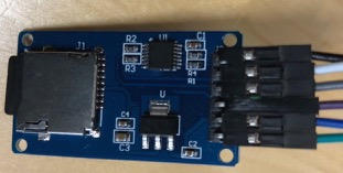
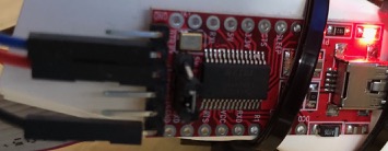
- In order to run the ZPU Evo iand it’s software in basic form on the QMTECH board you need 2 USB to Serial (ie. USB to Serial) adapters and you wire them up according to the pinout as is defined in the <zpu evo dir>/build/QMV_zpu.qsf file. Ensure the adapters are set to 3.3V. See Images section for colour coded wiring.
##============================================================ # UART #============================================================ set_location_assignment PIN_AA14 -to UART_RX_0 set_location_assignment PIN_AA15 -to UART_TX_0 set_location_assignment PIN_Y15 -to UART_RX_1 set_location_assignment PIN_AB18 -to UART_TX_1 - Open two Minicom/MobaXterm or equivalent serial consoles, setting the Serial port to one of the USB adapters in each. Setup the Baud Rate to 115200, with 8N1 formatting. Ensure auto line feed is enabled with Carriage Return.
- Connect the USB Blaster between the QMTECH board and the PC.
- Connect an SD Card Reader (ie. SD Card Reader) to the QMTECH board according to the pinout as is defined in the <zpu evo dir>/build/QMV_zpu.qsf file. See Images section for colour coded wiring.
##============================================================ # SD CARD #============================================================ set_location_assignment PIN_Y17 -to SDCARD_MISO[0] set_location_assignment PIN_AA18 -to SDCARD_MOSI[0] set_location_assignment PIN_AA20 -to SDCARD_CLK[0] set_location_assignment PIN_Y20 -to SDCARD_CS[0] - Insert the SD card created in the Software build above.
- Open the Quartus Programmer (ie. Quartus Prime -> Tools -> Programmer), select the sof file via ‘Add File’ which will be in the directory <zpu evo dir>/build/QMV_zpu.sof (QMV_EVO.sof if build was via Makefile) and setup the hardware via ‘Hardware Setup’.
- Program the FPGA via ‘Start’ and on success, in the serial terminal window you will see the ZPUTA sign on message.
Repository Structure
The GIT Repository is organised as per the build environment shown in the tables below.
RTL
| Folder | RTL File | Description |
|---|---|---|
| <root> | zpu_soc_pkg.tmpl.vhd | A templated version of zpu_soc_pkg.vhd used by the build/Makefile to configure and make a/all versions of the SoC. |
| zpu_soc_pkg.vhd | The SoC configuration file, this enables/disables components within the SoC. | |
| zpu_soc.vhd | The SoC definition and glue logic between enabled components. | |
| cpu/ | zpu_core_evo.vhd | The ZPU Evo CPU. |
| zpu_core_flex.vhd | The ZPU Flex CPU re-factored to keep the same style as the Evo and additional hardware debug output added. | |
| zpu_core_medium.vhd | The ZPU Medium (4) CPU re-factored to keep the same style as the Evo and additional hardware debug output added. | |
| zpu_core_small.vhd | The ZPU Small CPU re-factored to keep the same style as the Evo and additional hardware debug output added. | |
| zpu_pkg.vhd | The CPU configuration, bus address width etc. | |
| zpu_uart_debug.vhd | A hardware debug serializer to output runtime data to a connected serial port. | |
| devices/sysbus | BRAM | Block RAM RTL |
| intr | Interrupt Controller | |
| ps2 | PS2 Keyboard/Mouse Controller | |
| RAM | Dual Port RAM | |
| SDMMC | SD Controller | |
| spi | Serial Peripheral Interface Controller | |
| timer | Timer | |
| uart | Full duplex cached UART Controller | |
| devices/WishBone | I2C | I2C Controller |
| SRAM | Encapsulated Byte Addressable BRAM | |
| SDRAM | Byte Addressable 32Bit SDRAM Controller | |
| build | CYC1000 | Quartus definition files and Top Level VHDL for the Trenz Electronic CYC1000 Cyclone 10LP development board. |
| E115 | Quartus definition files and Top Level VHDL for the Cyclone IV EP4CE115 DDR2 64BIT development board. | |
| QMV | Quartus definition files and Top Level VHDL for the QMTech Cyclone V development board. | |
| DE10 | Quartus definition files and Top Level VHDL for the Altera DE10 development board as used in the MiSTer project. | |
| DE0 | Quartus definition files and Top Level VHDL for the Altera DE0 development board. | |
| Clock_* | Refactored Altera PLL definitions for various development board source clocks. These need to be made more generic for eventual inclusion of Xilinx fabric. |
Quartus Prime in Docker
Installing Quartus Prime can be tedious and time consuming, especially as the poorly documented linux installation can lead to a wrong mix or missing packages which results in a non-functioning installation. To ease the burden I have pieced together a Docker Image containing Ubuntu, the necessary packages and Quartus Prime 13.0sp1, 13.1 and 17.1.1.
-
Clone the repository:
 cd ~
 git clone https://github.com/pdsmart/zpu.git
 cd zpu/docker/QuartusPrime
Current configuration will build a Lite version of Quartus Prime. If you want to install the Standard version, before building the docker image:
 Edit:        zpu/docker/QuartusPrime/Dockerfile.17.1.1
 Uncomment:   '#ARG QUARTUS=QuartusSetup-17.1.0.590-linux.run'
 Comment out: 'ARG QUARTUS=QuartusLiteSetup-17.1.0.590-linux.run'.
If you have a license file:
 Copy: <your license file> to zpu/docker/QuartusPrime/files/license.dat
 Edit:  zpu/docker/QuartusPrime/run.sh
 Change: MAC_ADDR="02:50:dd:72:03:01" so that is has the MAC Address of your license file.
Build the docker image:
docker build -f Dockerfile.17.1.1 -t quartus-ii-17.1.1 --build-arg user_uid=`id -u` --build-arg user_gid=`id -g` --build-arg user_name=`whoami` .For Quartus Prime 13.0.1 and 13.1 replace 17.1.1 with the necessary version. Quartus Prime 13.0.1 supports the older Cyclone devices.
-
Setup your X DISPLAY variable to point to your xserver:
 export DISPLAY=<x server ip or hostname>:<screen number or :<screen number>>
 # ie. export DISPLAY=192.168.1.1:0
On your X server machine, issue the command:
xhost + # or xhost <ip of docker host> to maintain security on a non private network. -
Setup your project directory accessible to Quartus.
Edit: zpu/docker/QuartusPrime/run.sh Change: PROJECT_DIR_HOST=<location on your host you want to access from Quartus Prime> Change: PROJECT_DIR_IMAGE=<location in Quartus Prime running container to where the above host directory is mapped> # ie. PROJECT_DIR_HOST=/srv/quartus PROJECT_DIR_IMAGE=/srv/quartus -
Run the image using the provided bash script ‘run.sh’. This script
./run.shThis will start Quartus Prime and also an interactive bash shell.
On first start it currently asks for your license file, click ‘Run the Quartus Prime software’ and then OK. It will ask you this question everytime you start a new container albeit Im looking for a work around.
The host devices are mapped into the running docker container so that if you connect a USB Blaster it will be seen within the Programmer tool. As part of the installation I install the udev rules for USB-Blaster and USB-Blaster II as well as the Arrow USB-Blaster driver for use with the CYC1000 dev board. -
To stop quartus prime:
 # Either exit the main Quartus Prime GUI window via File->Exit
 # or
 docker stop quartus
Images
Images of QMTECH Cyclone V wiring
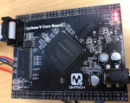
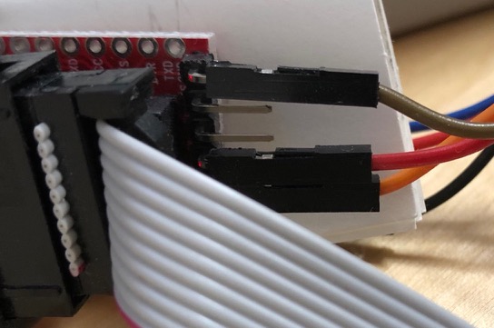
Above are the wiring connections for the QMTECH Cyclone V board as used in the Build section, colour co-ordinated for reference.
Images of ZPUTA on a ZPU EVO CPU
ZPU Performance
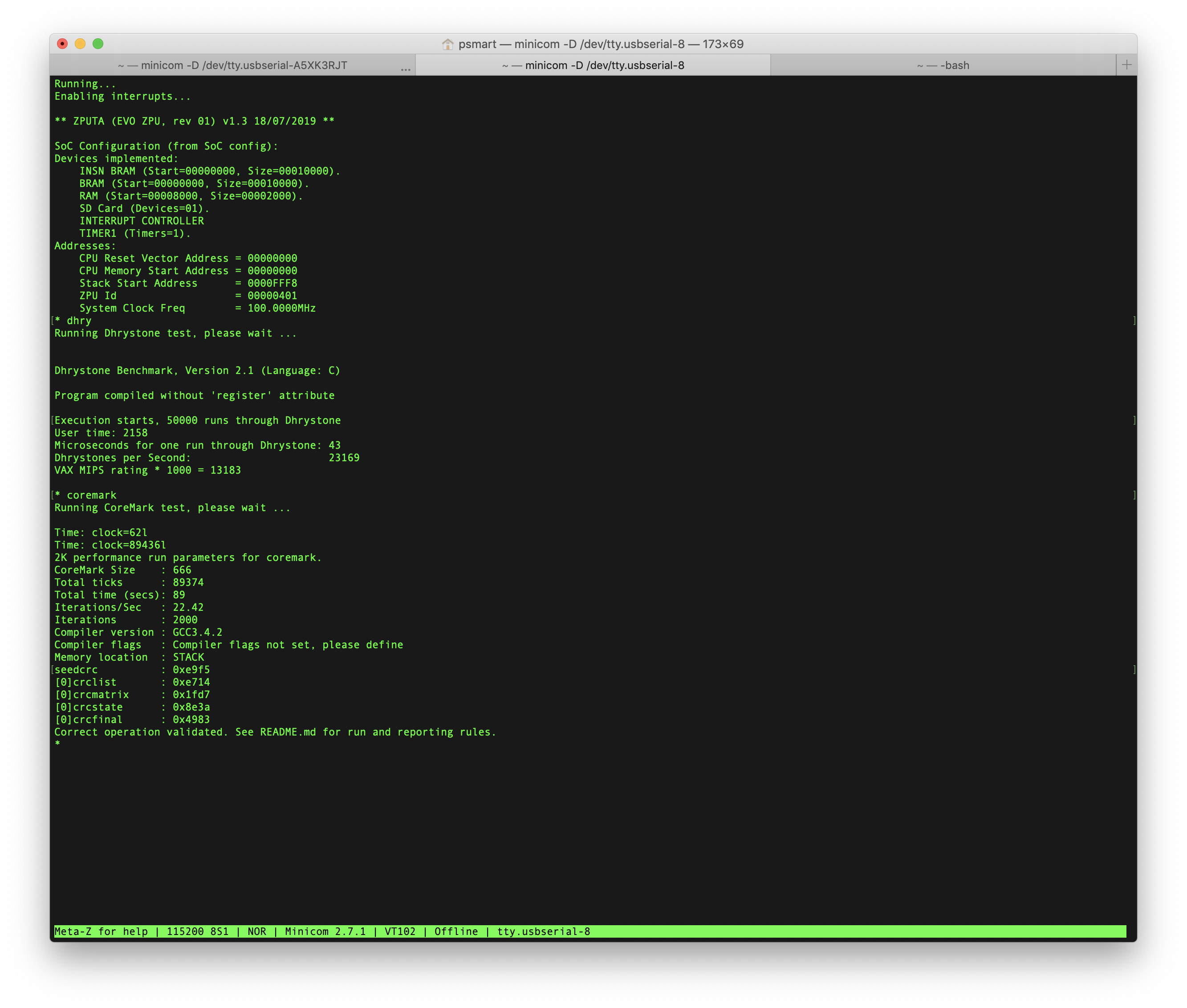 Dhrystone and CoreMark performance tests of the ZPU Evo CPU. Depending on Fabric there are slight variations, these tests are on a Cyclone V CEFA chip, on a Cyclone IV CE I7 the results are 13.2DMIPS for Dhrystone and 22.2 for CoreMark.
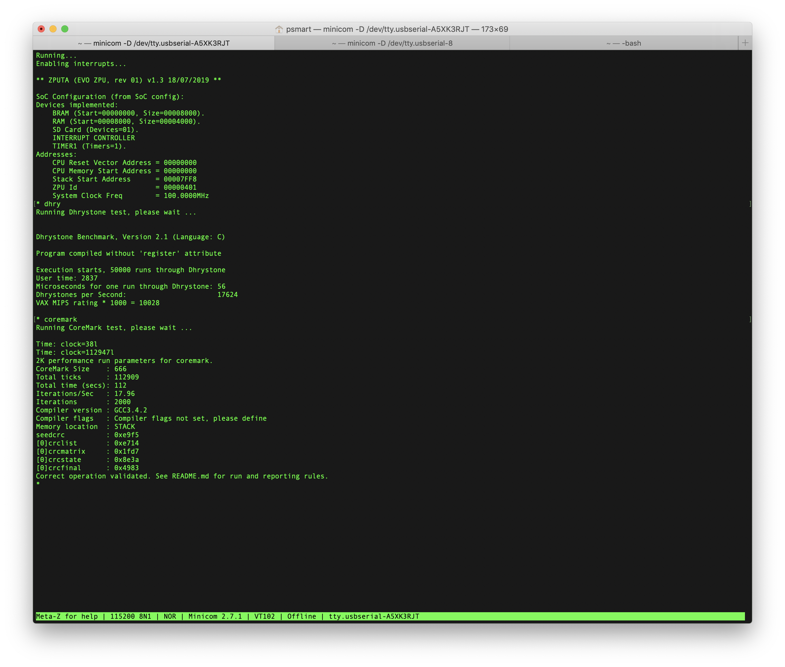 Same test as above but on a Cyclone 10LP with limited resources, only using single port memory with no instruction bus, the results are 10.0DMIPS for Dhrystone and 17.96 for CoreMark.
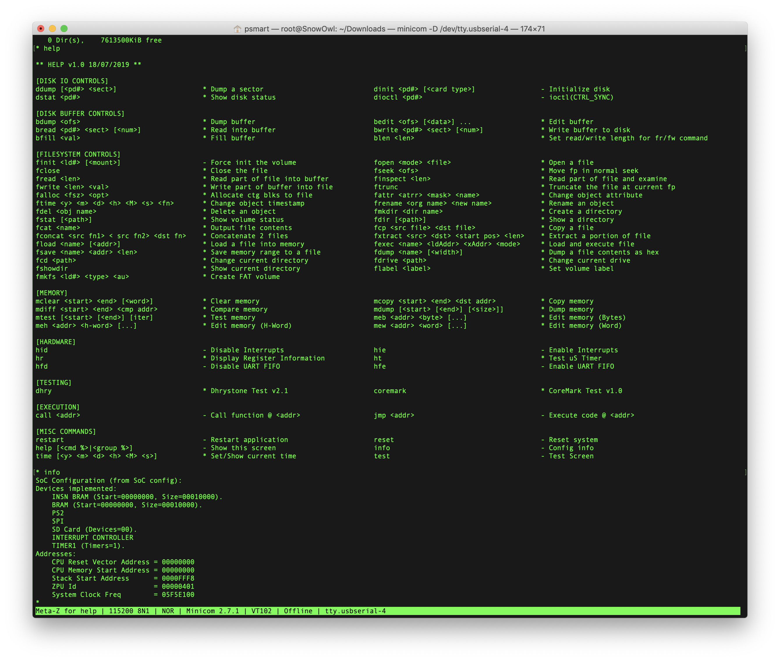 Help screen for ZPUTA, help in this instance is an applet on the SD Card. A * before the description indicates the command is on SD, a - indicates the command is built-in.
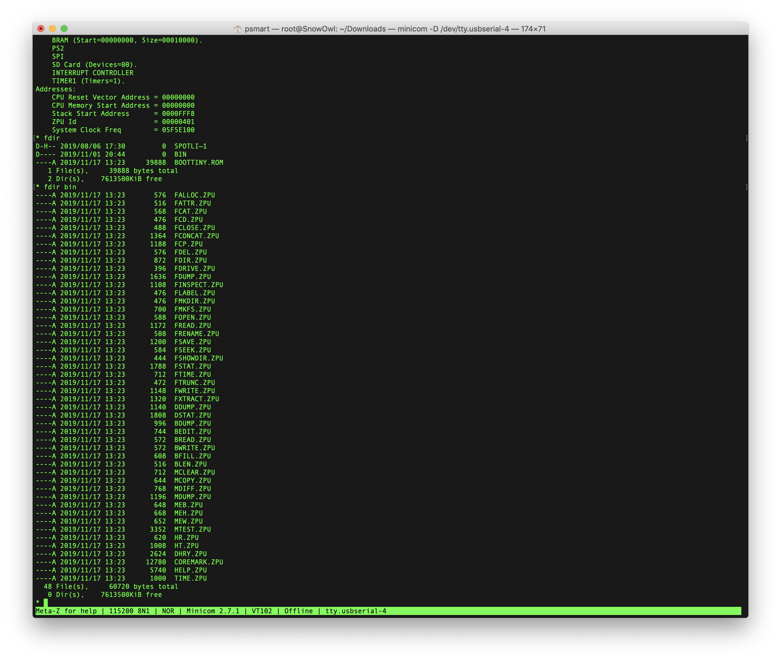 SD Directory listings of all the compiled applets.
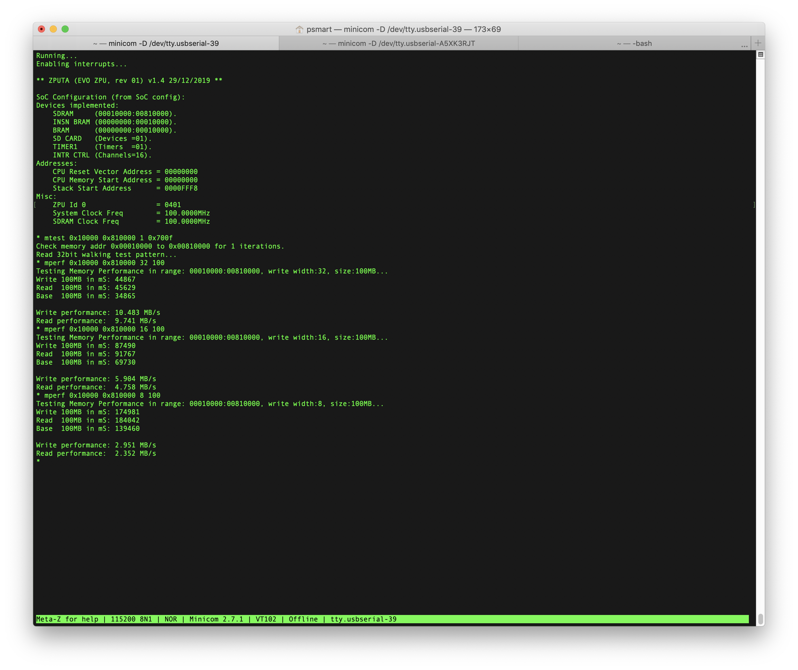
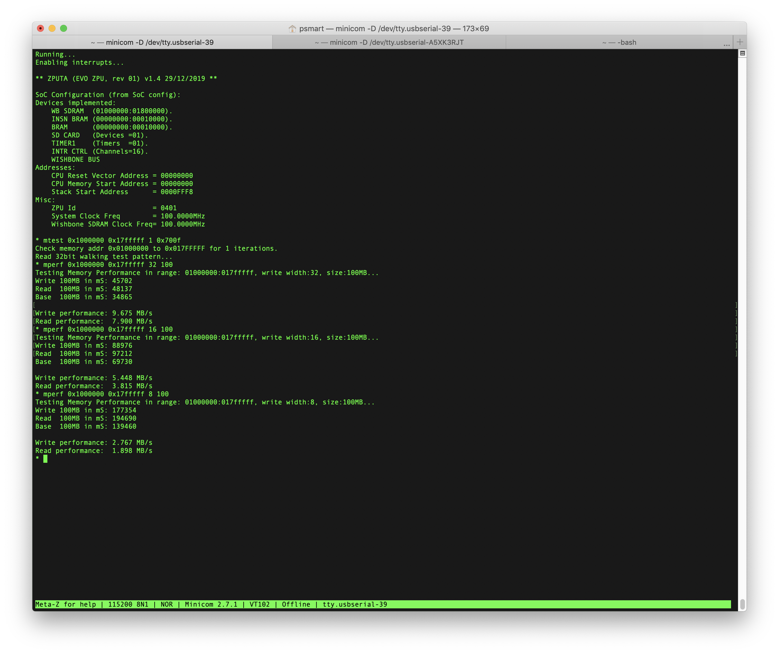
SDRAM Performance
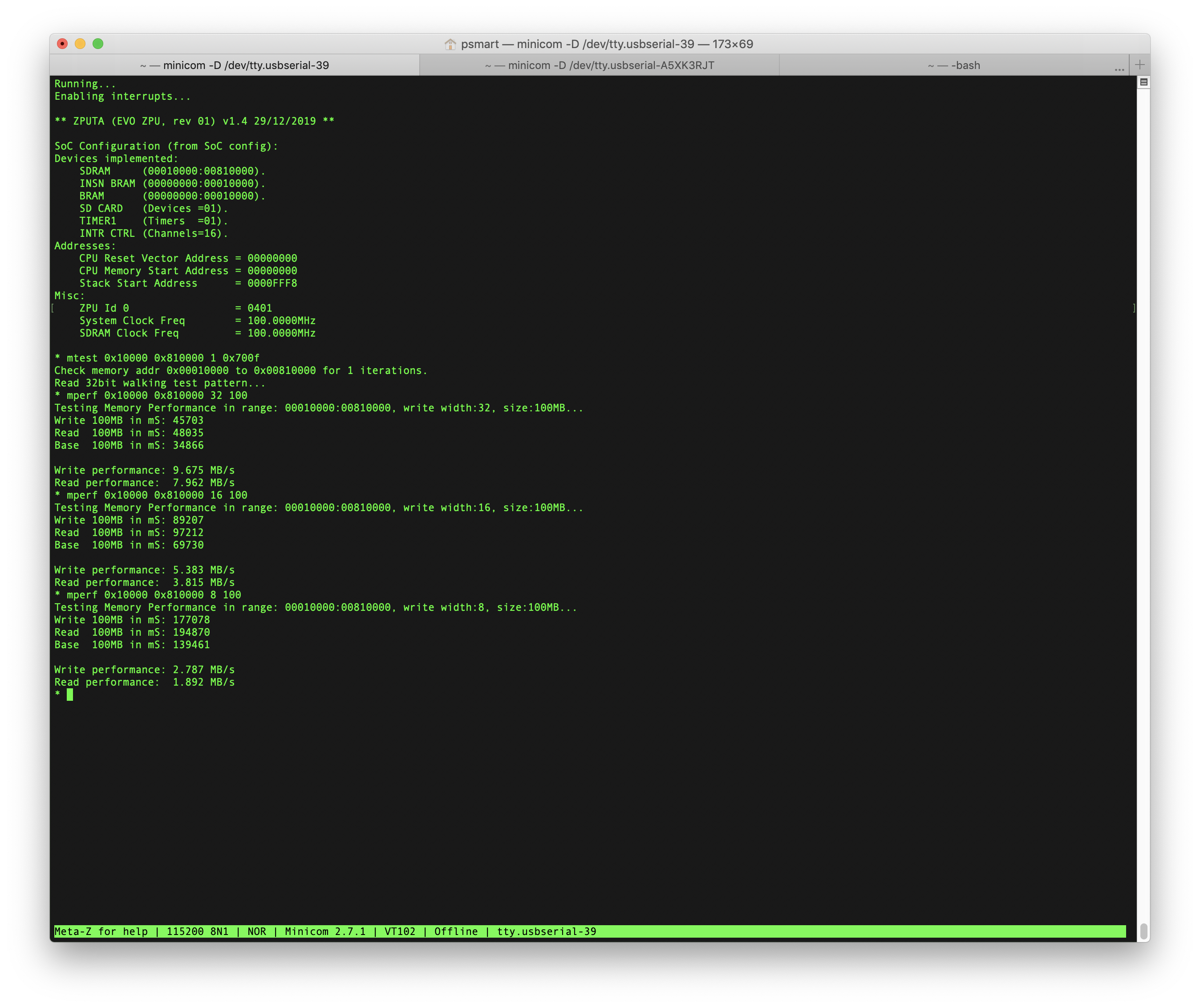 SDRAM operating over the SYSBUS and with no cache. Not quite true memory performance as the ZPU makes several stack operations for a memory read/write, ie. IM <address>, IM , STORE for a write which would entail upto 11 instruction reads (3 cycles on the Evo) and two stack writes.
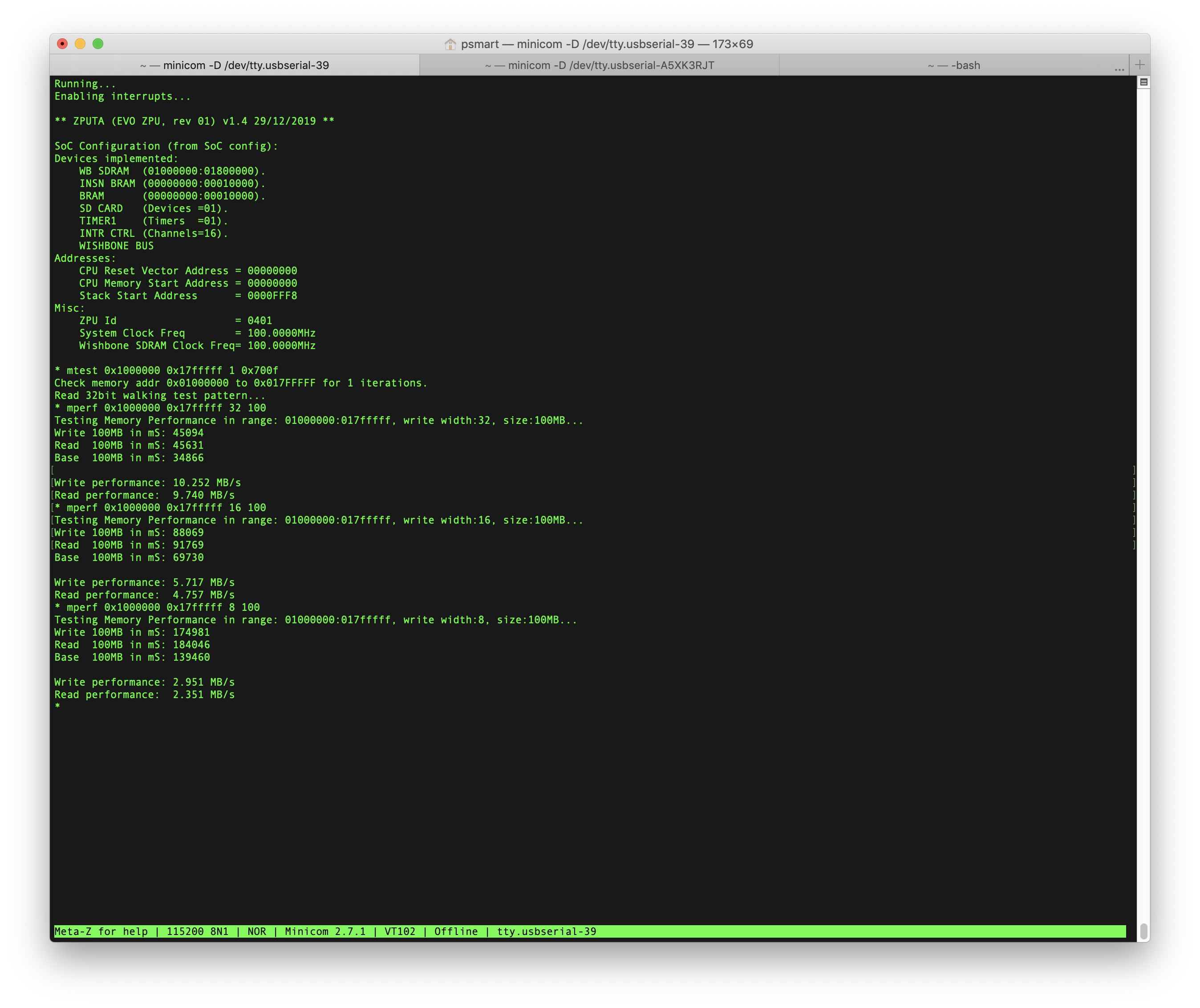
 SDRAM operating over the SYSBUS with full page cache per bank for read and write-thru cache for write.
 SDRAM operating over the WishBone Bus and with no cache.
 SDRAM operating over the WishBone Bus with full page cache per bank for read and write-thru cache for write.
Links
| Recommended Site |
|---|
| Original Zylin ZPU repository |
| Original Zylin GCC v3.4.2 toolchain |
| Flex ZPU repository |
| ZPUino and Eco System |
| Wikipedia ZPU Reference |
Credits
Where I have used or based any component on a 3rd parties design I have included the original authors copyright notice within the headers or given due credit. All 3rd party software, to my knowledge and research, is open source and freely useable, if there is found to be any component with licensing restrictions, it will be removed from this repository and a suitable link/config provided.
Licenses
The original ZPU uses the Free BSD license and such the Evo is also released under FreeBSD. SoC components and other developments written by me are currently licensed using the GPL. 3rd party components maintain their original copyright notices.
The FreeBSD license
Redistribution and use in source and binary forms, with or without modification, are permitted provided that the following conditions are met:
- Redistributions of source code must retain the above copyright notice, this list of conditions and the following disclaimer.
- Redistributions in binary form must reproduce the above copyright notice, this list of conditions and the following disclaimer in the documentation and/or other materials provided with the distribution.
THIS SOFTWARE IS PROVIDED ``AS IS’’ AND ANY EXPRESS OR IMPLIED WARRANTIES, INCLUDING, BUT NOT LIMITED TO, THE IMPLIED WARRANTIES OF MERCHANTABILITY AND FITNESS FOR A PARTICULAR PURPOSE ARE DISCLAIMED. IN NO EVENT SHALL THE ZPU PROJECT OR CONTRIBUTORS BE LIABLE FOR ANY DIRECT, INDIRECT, INCIDENTAL, SPECIAL, EXEMPLARY, OR CONSEQUENTIAL DAMAGES (INCLUDING, BUT NOT LIMITED TO, PROCUREMENT OF SUBSTITUTE GOODS OR SERVICES; LOSS OF USE, DATA, OR PROFITS; OR BUSINESS INTERRUPTION) HOWEVER CAUSED AND ON ANY THEORY OF LIABILITY, WHETHER IN CONTRACT, STRICT LIABILITY, OR TORT (INCLUDING NEGLIGENCE OR OTHERWISE) ARISING IN ANY WAY OUT OF THE USE OF THIS SOFTWARE, EVEN IF ADVISED OF THE POSSIBILITY OF SUCH DAMAGE.
The views and conclusions contained in the software and documentation are those of the authors and should not be interpreted as representing official policies, either expressed or implied, of the this project.
The Gnu Public License v3
The source and binary files in this project marked as GPL v3 are free software: you can redistribute it and-or modify it under the terms of the GNU General Public License as published by the Free Software Foundation, either version 3 of the License, or (at your option) any later version.
The source files are distributed in the hope that it will be useful, but WITHOUT ANY WARRANTY; without even the implied warranty of MERCHANTABILITY or FITNESS FOR A PARTICULAR PURPOSE. See the GNU General Public License for more details.
You should have received a copy of the GNU General Public License along with this program. If not, see http://www.gnu.org/licenses/.