 tranZPUter
Foreword
During testing of the tranZPUter v1.0 and with the advent of the RFS v2.0 upgrade with CP/M it was noticed that the tranZPUter should be updated so that the Z80 had additional memory and was able to run at higher clock frequencies. It should also run independent of the controlling IO processor, ie. the ZPU Evo on FPGA fabric or the K64F.
V1.0 of the tranZPUter had design restrictions which in all honesty make the project much harder to complete, for example, because of my lack of experience soldering BGA (Ball Grid Array) IC's, I chose the next best thing, a pre-fab FPGA board, the CYC1000 with the FPGA already soldered. This device and all other possibilities for the given size and FPGA ALM requirements had too few general I/O pins. This meant that multiplexing had to be used with tri-state register latches. KISS comes back to mind, Keep It Simple Stupid! So in order to further the concept and design I took a step back, looked at what was needed at the Z80 side to realise the CP/M requirements and looked at what was needed for the controlling IO Processor. I then furthered the design and concept with the tranZPUter SW sub-project before returning to the original tranZPUter and recommencing with v2.0 of the design.
Overview
Besides providing more powerful and alternative CPU's and memory, the FPGA can also act as a Floppy Drive, Hard Drive etc using the connected SD Card and provide a menu system by overlaying the video memory when invoked.
This design is still a work in progress, I initially stopped development to advance the ZPU Evo SDRAM controller which I had been putting off for a while. The SDRAM is critical as the Cyclone 10LP on the CYC1000 has limited BRAM, only enough for the cache and IOCP Bootloader. Many features have been tested and the schematic/pcb made, it is just a matter of furthering the VHDL now that the SDRAM controller works and to develop the C/C++ code to provide the menu/SD services (already done in the ZPU code base).
I chose the CYC1000 as the FPGA solution as I am not happy soldering BGA devices, also at US$30 it is quite a cost effective choice. For software minded people, it is not that difficult to use a Pi Zero W or similar (the tranZPUter-SW sub-project made use of the Cortex-M4 ARM based K64F) in place of the CYC1000 just a reworking of the PCB and interface logic.
As the design replaces a Z80 in-situ it is not limited to the MZ80A but can be used in any Z80 based computer with the right software.
The tranZPUter
To provide different CPU's it is just a matter of mapping in VHDL the softcore CPU signals to the MZ80A bus via this designs interface. The program memory could either be that on the MZ80A or the faster SDRAM. ie. There is no real need to use the MZ80A memory when using a softcore CPU. In my SharpMZ Emulator I run a Z80 at 112MHz using FPGA BRAM but tests show at least 128MHz is sustainable, thus a softcore Z80 CPU running at 128MHz with 48K BRAM slowing down only for MZ80A peripheral access would see a 64x boost in program run, which for say CP/M or database use is very desirable.
In the gallery are pictures of the current design and files uploaded onto github are relatively stable, WIP files wont be uploaded as they are in constant flux.
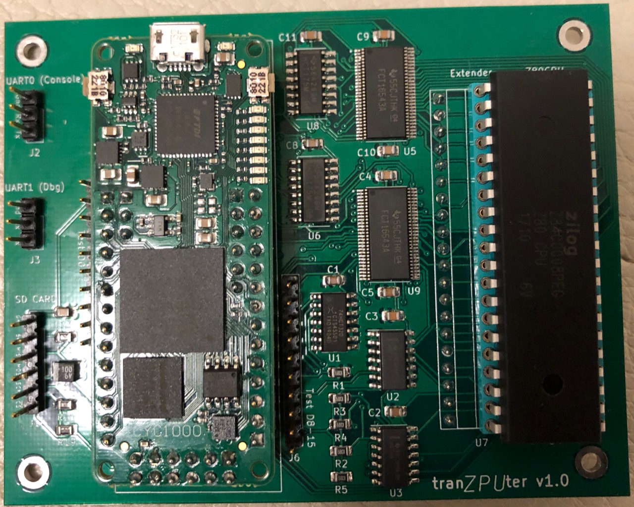
v1.0 Hardware
In this design, the bus mastering is used in a similar vein, taking control of the Z80 bus to transfer data between main memory and an SD Card or between the I/O processor and the Video display buffer for presentation of menu's. It is also used where a soft processor completely idle's the hard Z80 and acts as the main computer CPU. ie. using a soft T-80 ZPU CPU, it can process applications at 128MHz in local memory and slow down to access I/O and the Video buffer on the host machine.
The design centres around lifting the original Z80 onto a daughter card and rerouting several of its signals such that they can be controlled as needed. The core of the design is an FPGA, the Altera Cyclone 10LP on a mini development board made by Trenz Electronics. This could quite easily be a Raspberry Pi or Teensy 3.6 but the aim of this project is to design electronic hardware in an FPGA using VHDL and making use of the ZPU Processor I have been working on in a seperate project.
The choice of the Trenz Electronic development board put a number of restrictions on the design in so much as it only provides limited I/O facilities. There were not so many other choices of pre-built FPGA development boards with the same size and features to choose from and designing an FPGA directly into the design from project onset was considered too much a risk because my experience with BGA (Ball Grid Array) packaging and soldering of them was almost zero (I have reballed existing chips but those were working designs!).
As there were limited I/O facilities, I had to make use of two 16bit tri-state buffer latches in an addressed mode rather than a 1:1 mode. ie. The Z80 Data, Address and Control lines eminating out of the FPGA have to be 'set' one word at a time, ie. write data to latch, write address to latch, write control signals to latch etc. This slows down the speed at which the FPGA can control the Z80 host (to be honest, a 100MHz FPGA can run 50 operations and still match the 2MHz original bus speed) and complicates the logic by requirement of FSM's in VHDL.
It is further complicated by the fact that the signals controlling the latches have themselves to be written in an addressed mode rather than direct, again due to lack of I/O facilities on the FPGA board. Thus in the schematic above you can see IC U6 & U8 being written to via the common 16bit data bus (shared with the latches) and clocked by a single output signal from the FPGA. A delay line is used such that a write to the latch is performed by signal CYC_CTL/RST going high, this reaches the latch ~8ns after the same signal connected to the Master Reset goes high, thus clocking in the data. The latches are reset when CYC_CTL/RST goes low and this is enough to control the 16 bit latches U5 & U9. ie. to write a 16bit word into U5 the procedure would be:
CYC_CTL/RST low
Set CYC_D0:7 to 0x02 (ADDR_LE active, low)
Set CYC_CTL/RST high, data on CYC_D0:7 is latched into U6/U8 and ADDR_LE goes active enabling transfer of data on CYC_D0:15 into U5 registers (latches on the rising edge of ADDR_LE).
Set required data on CYC_D0:15 that will be passed across to the Z80 BUS.
Set CYC_CTL/RST low, ADDR_LE goes inactive (high) and the data on CYC_D0:15 is latched into U5
v1.0 Schematic
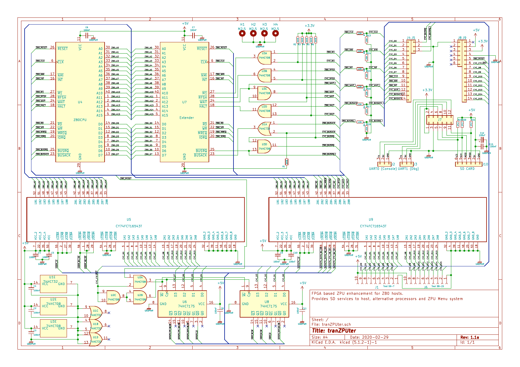
Once the FPGA FSM is fine tuned, the actual write and read to/from the Z80 bus will be transparent but it is overly complicated as mentioned due to lack of I/O on the Trenz development board.
Postface
I abandoned work on v1.0 of the FPGA based tranZPUter for 2 reasons:
1. the Z80 circuit needed enhancements to support CP/M and other software,
2. the use of the Trenz CYC1000 was a bad choice, with its limited I/O resources it made the design overly complicated.
Work on the tranZPUter continues with the tranZPUter SW (SoftWare) and design know how will be fed back into the inteded v2.0 of the tranZPUter.
v2.0 Hardware
To this aim, I procured some high end FPGA's (not the latest generation to reduce cost) which provide 110K Logic Elements and over 500KB BRAM and commenced a design from the knowledge gained writing the ZPU Evo, the tranZPUter SW and the FPGA based Video Module.
This section outlines the design which is still in-progress.
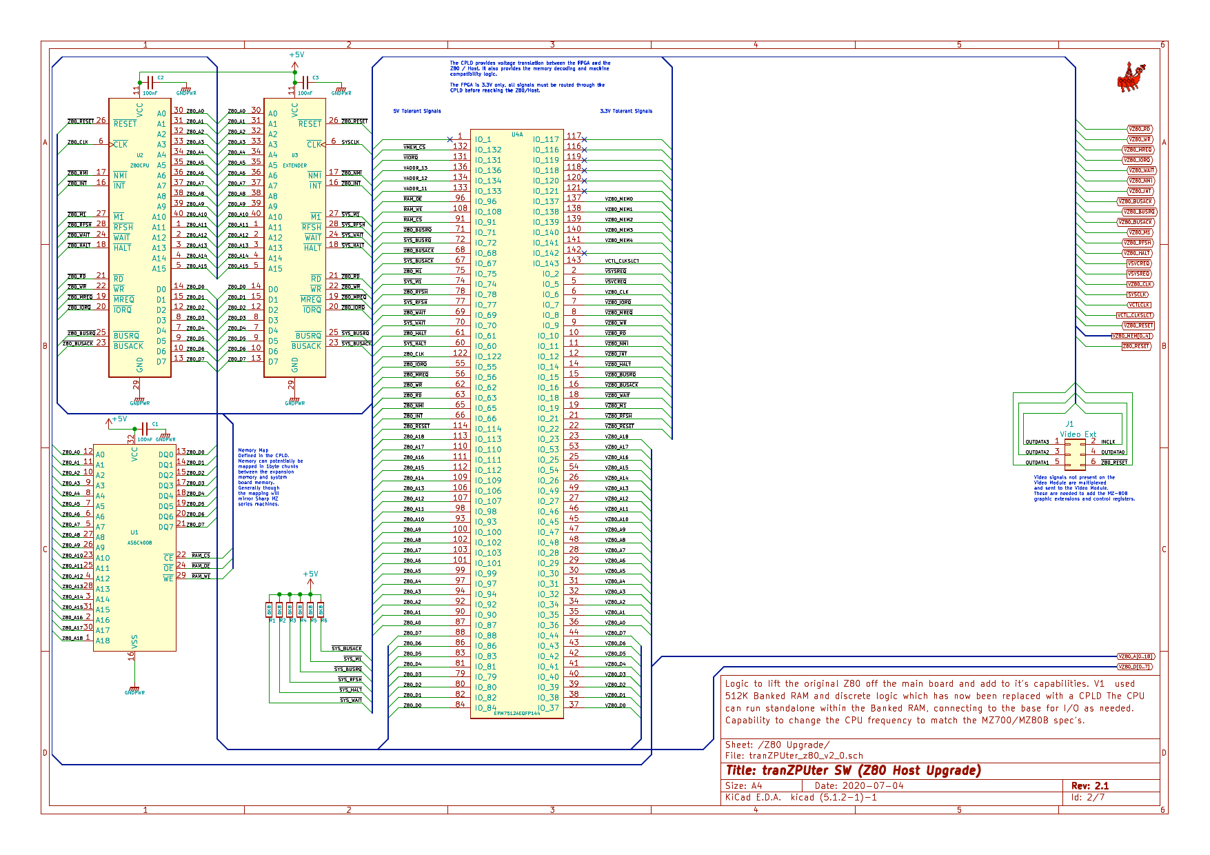
v2.0 Z80 Upgrade Schematic
v2.0 FPGA Schematic
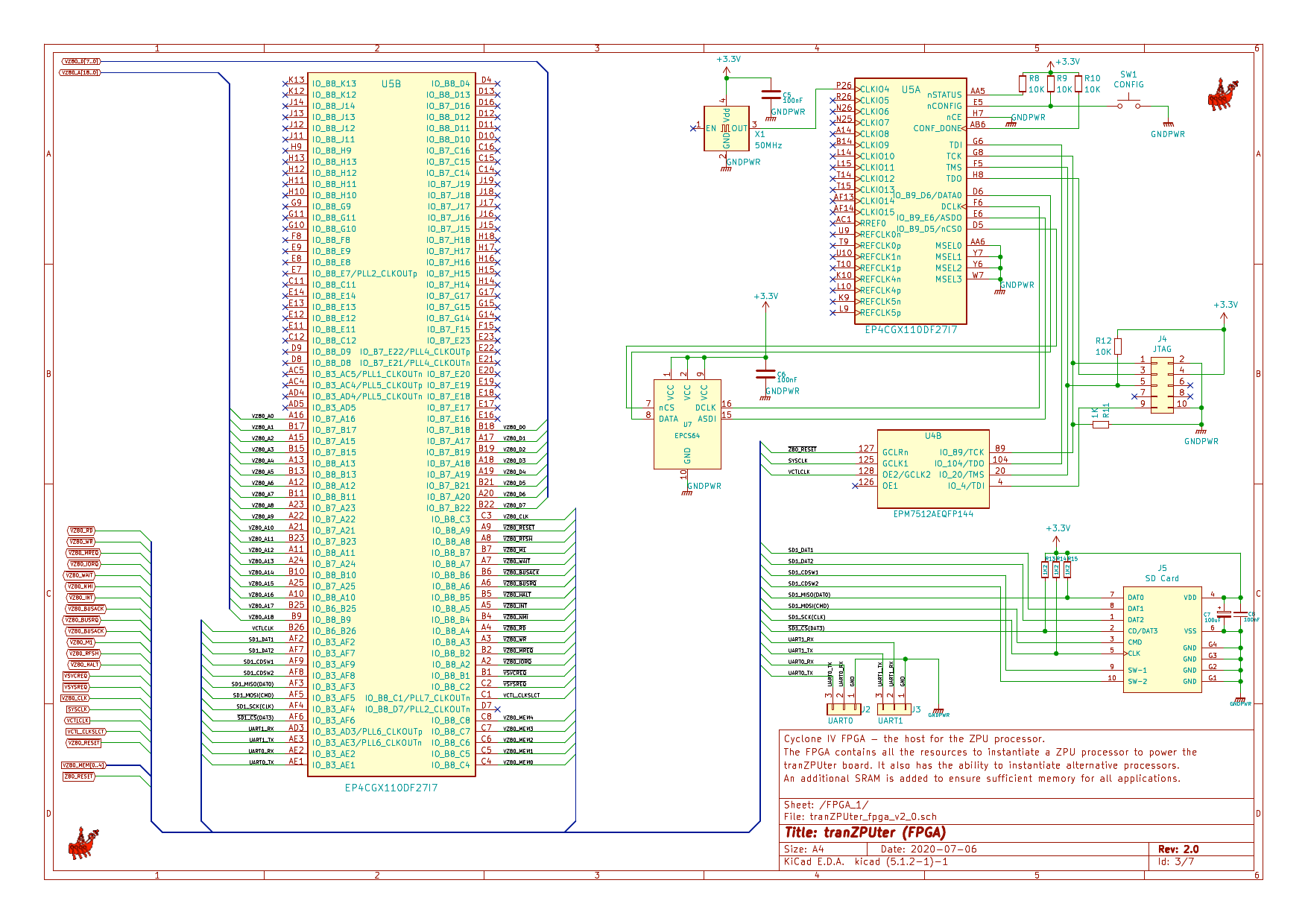
Version 2.0 takes a leap forward from v1.0 in that it uses a much larger sized BGA FPGA instead of the Cyclone 10 LP found on the CYC1000 board. This device, the Cyclone IV CGX75 offers 110K Logic Elements and over 500KB BRAM, thus allowing many possibilities.
v2.0 FPGA RAM Schematic
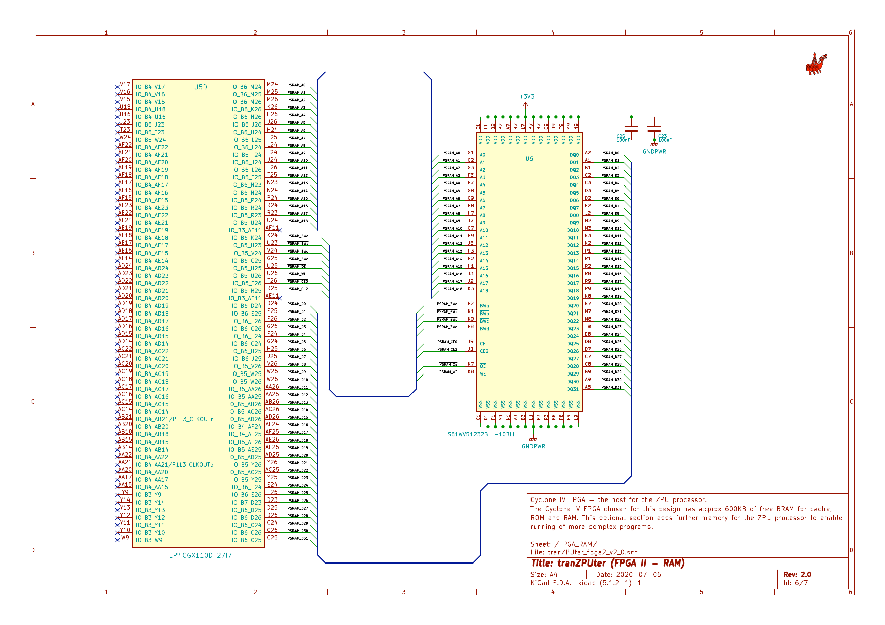
Version 2.0 will utilise my ZPU Evo design and additional memory is required to match the K64F in order to keep a level playing field in terms of available memory for zOS and its applications. The memory chosen is 10ns static RAM which will allow the ZPU to run without the need for L2 cache.
v2.0 PSU and Decoupling Schematics
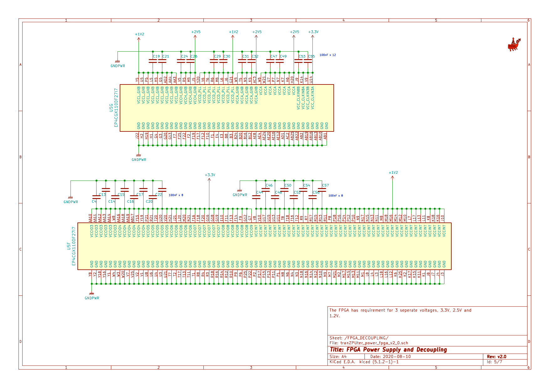
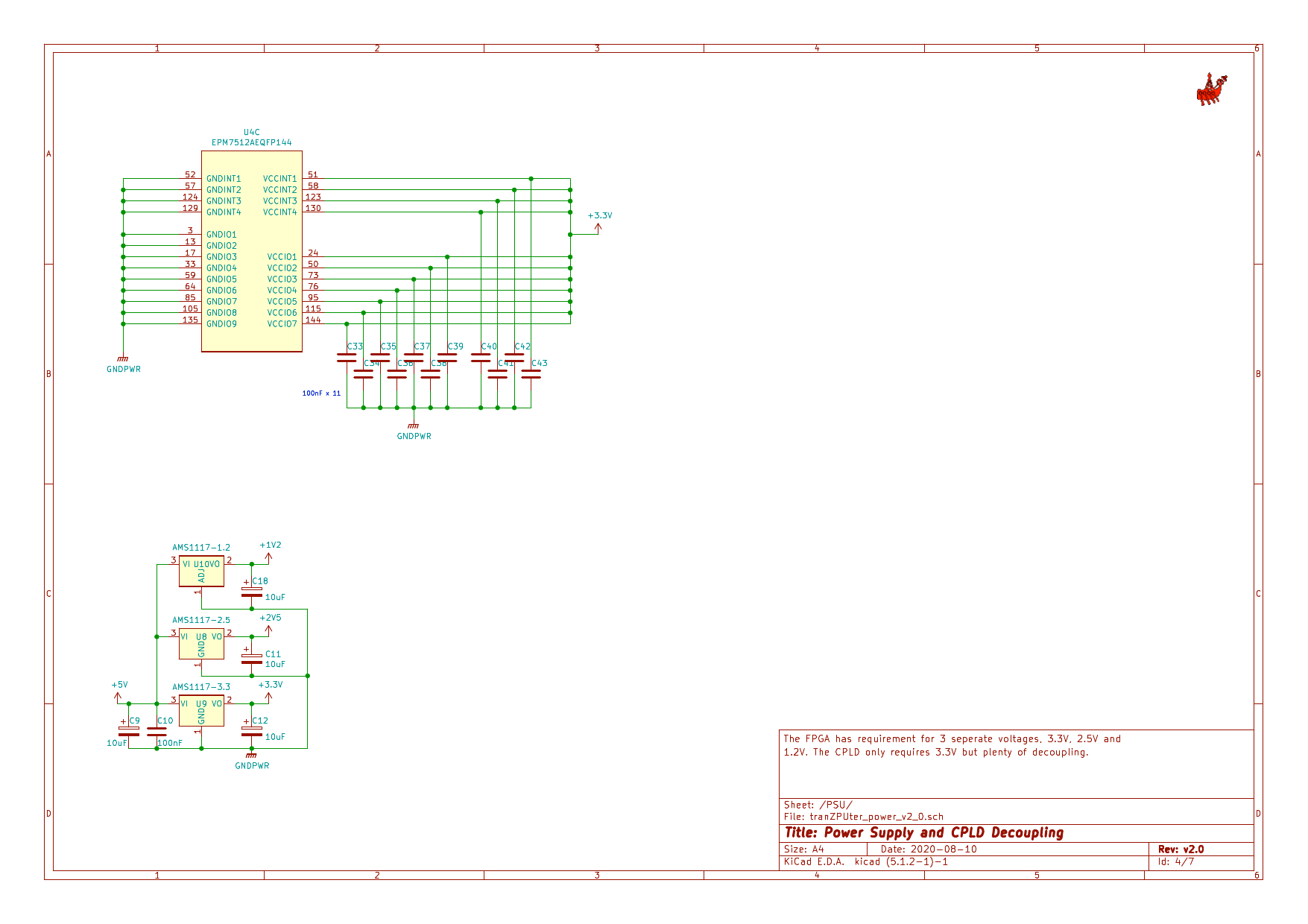
Using a larger FPGA brings with it greater demands on the power supply, especially decoupling, hence the need for a lot of decoupling capactors, inline with the Altera PDN Design Tool v1.1 for the Cyclone IV.
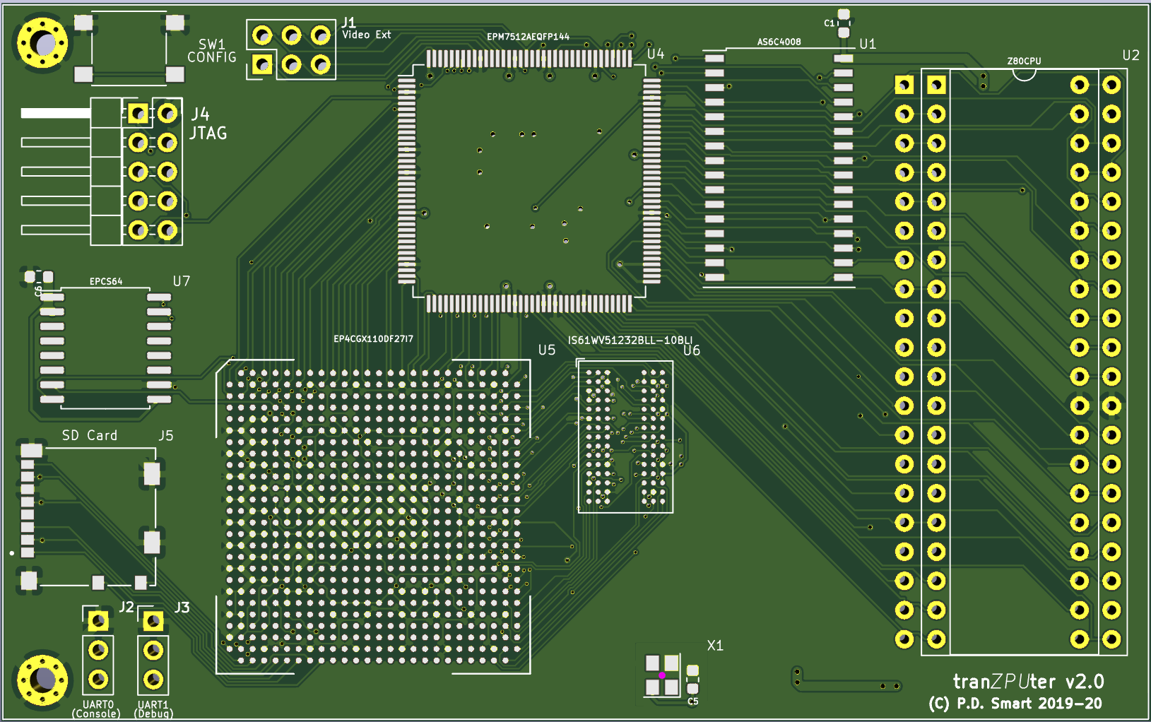
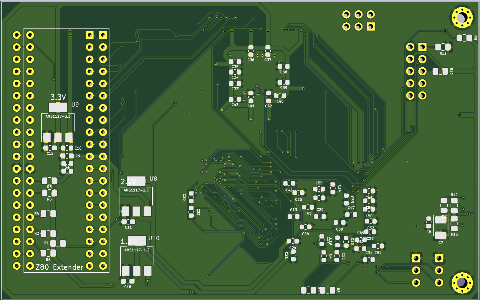
v2.0 PCB
Version 2.0 of the PCB compacts the design quite a bit building on the tranZPUterSW developments.
The board below is the Kicad image of the PCB under design. This board isnt yet finished due to the simple fact I hit upon new ideas whilst working on this board and started advancing v2.1 of the design. Im not sure if I will complete v2.0 and get it manufactured, it depends on the v2.1 design. It is here mainly for reference in respect of the development stages of the tranZPUter project.
Credits
Where I have used or based any component on a 3rd parties design I have included the original authors copyright notice. All 3rd party software, to my knowledge and research, is open source and freely useable, if there is found to be any component with licensing restrictions, it will be removed from this repository and a suitable link/config provided.
Licenses
This design, hardware and software, is licensed under the GNU Public Licence v3.
The Gnu Public License v3
The source and binary files in this project marked as GPL v3 are free software: you can redistribute it and-or modify it under the terms of the GNU General Public License as published by the Free Software Foundation, either version 3 of the License, or (at your option) any later version.
The source files are distributed in the hope that it will be useful, but WITHOUT ANY WARRANTY; without even the implied warranty of MERCHANTABILITY or FITNESS FOR A PARTICULAR PURPOSE. See the GNU General Public License for more details.
You should have received a copy of the GNU General Public License along with this program. If not, see http://www.gnu.org/licenses/.