 MZ-80A Rom Disk — Developer's Guide
RomDisk Developer's Guide
This guide is a detailed walkthrough of the Sharp MZ-80A RomDisk PCB firmware source code and development environment. It explains Z80 assembly language concepts for developers who may not be familiar with the language, describes the RomDisk-specific bank-switching mechanism in depth, walks through every source module, and shows how to add new commands, add new SPI hardware variants, and debug firmware running on real hardware.
The RomDisk firmware is a variant of the ROM Filing System (RFS). Unless noted otherwise, all descriptions here apply to builds with
BUILD_ROMDISK EQU 1 in rfs_definitions.asm. For hardware architecture and PCB construction details see the RomDisk hardware page. For user-facing operation see the RFS User Manual.
Introduction to Z80 Assembly for Non-Assembly Programmers
The entire RomDisk firmware is written in Z80 assembly language — the native instruction language of the Zilog Z80 processor used in the Sharp MZ series. Unlike high-level languages, assembly maps almost directly to the physical hardware: every instruction translates to one or a few bytes that the CPU executes directly.
Registers
The Z80 has no "variables" — instead it has a small set of registers (fast storage locations inside the CPU). The most commonly used ones in RFS:
| Register | Size | Role |
|---|---|---|
| A | 8-bit | Accumulator — the primary register for arithmetic, logic, and I/O operations. Almost every instruction involves A. |
| B, C | 8-bit | General purpose. BC together forms a 16-bit pair, commonly used as a loop counter or byte count. |
| D, E | 8-bit | General purpose. DE together is a 16-bit pair, commonly used as a source or destination pointer. |
| H, L | 8-bit | General purpose. HL together is the main 16-bit memory pointer — most memory read/write instructions use HL. |
| IX, IY | 16-bit | Index registers — used for base+offset memory addressing. Slower than HL but convenient for structured data. |
| SP | 16-bit | Stack Pointer — points to the top of the call stack. PUSH and POP use SP automatically. |
| PC | 16-bit | Program Counter — the address of the current instruction. Incremented automatically; modified by jumps and calls. |
| F | 8-bit | Flags register — individual bits set by arithmetic operations: Z (zero), C (carry), S (sign), P/V (parity/overflow). |
LD dest, src— Load (copy) data.LD A, Bcopies B into A.LD A, (HL)reads the byte at the memory address held in HL into A.LD (0x1200), Awrites A to memory address 0x1200.CALL addr— Call a subroutine. Pushes the return address (next instruction) onto the stack and jumps toaddr. Equivalent to a function call.RET— Return from subroutine. Pops the return address off the stack and jumps to it.JP addr— Unconditional jump toaddr.JP Z, addrjumps only if the Zero flag is set (i.e. the last operation produced zero).JR offset— Short relative jump (−128 to +127 bytes). Faster and more compact than JP for nearby branches.DJNZ offset— Decrement B and jump if Not Zero. The canonical Z80 loop instruction:LD B, 10 / LOOP: ... / DJNZ LOOPrepeats 10 times.ADD A, n— Add n to A.SUB nsubtracts.AND n,OR n,XOR n— bitwise logic on A.IN A, (port)— Read from I/O port into A.OUT (port), A— write A to I/O port. These are how the Z80 communicates with hardware (the WD1773 floppy controller, SPI shift registers, bank latch, etc.).PUSH rr / POP rr— Save/restore a 16-bit register pair to/from the stack.EI / DI— Enable / Disable interrupts. Code that must not be interrupted (e.g. time-critical tape operations) is wrapped between DI and EI.
The Z80 offers several ways to specify where data comes from or goes to:
GLASS Assembler Syntax
- Immediate:
LD A, 42— the value is embedded in the instruction bytes themselves. - Register:
LD A, B— data comes from or goes to a register. - Indirect (via HL):
LD A, (HL)— HL contains a memory address; data is read from that address. - Extended (direct address):
LD A, (0x1200)— the address is a literal 16-bit constant in the instruction. - Indexed:
LD A, (IX+5)— IX holds a base address; 5 is added to get the effective address. Used in RFS for accessing fields within fixed-format data structures.
RFS uses the GLASS Z80 assembler (bundled as
tools/glass.jar). Key syntax features:
- Comments begin with
;— everything to the right of a semicolon is ignored. - Labels are identifiers followed by
:. A label at the start of a line names the address of the next instruction. EQUdefines a constant:BELL EQU 007H— the assembler replaces every occurrence of BELL with 0x07.DB(Define Byte) inserts raw bytes:DB 0x41, 0x42emits two bytes. Used for strings, lookup tables, and command table entries.DW(Define Word) inserts 16-bit little-endian values:DW HANDLERemits the address of the HANDLER label.ORG addrsets the assembly origin — subsequent code is assembled as if it lives ataddr.INCLUDE "file.asm"textually includes another file at the current position.IF / ENDIFconditional assembly:IF HW_SPI_ENA = 1 ... ENDIF— the enclosed instructions are only assembled when the condition is true. This is how RFS selects between hardware SPI, software SPI, and parallel-port SPI from one source tree.
Source Tree
| Path | Contents |
|---|---|
README.md |
Top-level project overview |
README_CPM.md |
CP/M-specific notes |
schematics/ |
KiCad schematics for PCB v1.1, v2.0, v2.1 |
pcb/ |
KiCad PCB layout files |
software/RFS/ |
RFS firmware submodule (also at /dvlp/Projects/RFS) |
software/RFS/asm/ |
All Z80 assembly source files |
software/RFS/asm/include/ |
Shared configuration and utility includes |
software/RFS/tools/ |
Build scripts and GLASS assembler (glass.jar) |
software/RFS/build.sh |
Top-level build script |
The assembly source files and their roles:
| File | Bank | Role |
|---|---|---|
rfs.asm |
User ROM Bank 0 | Entry point, command table, bank-switch stubs, jump table |
rfs_bank1.asm |
User ROM Bank 1 | Floppy disk controller |
rfs_bank2.asm |
User ROM Bank 2 | SD card controller (SPI driver, SDCFS) |
rfs_bank3.asm |
User ROM Bank 3 | Memory utilities (D, M, CP, T2SD, SD2T) |
rfs_bank4.asm |
User ROM Bank 4 | CMT (cassette tape) controller |
rfs_bank5.asm |
User ROM Bank 5 | Reserved / unused |
rfs_bank6.asm |
User ROM Bank 6 | Messages, help screen, ASCII↔Sharp character conversion |
rfs_bank7.asm |
User ROM Bank 7 | Memory test (R command), timer test (T command) |
rfs_mrom.asm |
Monitor ROM Bank 3 | MZF ROM scanning and loading (ROMDIR, ROMLOAD) |
cbios.asm |
Monitor ROM Bank 2 | CP/M CBIOS entry point table and ROM disk controller |
cbios_bank1–4.asm |
User ROM Banks 8–11 | CP/M CBIOS subsystems |
monitor_sa1510.asm |
— | SA-1510 Monitor ROM reference |
monitor_80c_sa1510.asm |
— | SA-1510 Monitor ROM (80-column variant) |
ipl.asm |
— | Initial Program Loader |
include/rfs_definitions.asm |
— | All configuration constants |
include/rfs_utilities.asm |
— | Shared utility macros |
include/macros.asm |
— | Assembler macro definitions |
include/cpm_definitions.asm |
— | CP/M CBIOS constants |
Configuration: rfs_definitions.asm
This is the central configuration file, included by every other source file via
Build Target and SPI Flags
INCLUDE "rfs_definitions.asm". Every assembly-time option is controlled here. The key sections:
; SPI hardware selection — exactly ONE must be 1:
HW_SPI_ENA    EQU 1    ; Hardware SPI on RomDisk v2+ PCB (74HCT595/165 shift registers)
SW_SPI_ENA    EQU 0    ; Software bit-bang SPI via Z80 I/O port bits
PP_SPI_ENA    EQU 0    ; Parallel printer port SPI (v1 boards only)

; Platform options:
FUSIONX_ENA   EQU 1    ; Include tranZPUter FusionX support
KUMA80_ENA    EQU 0    ; Target has Kuma 40/80 upgrade installed
VIDEOMODULE_ENA EQU 0  ; Target has 40/80 column colour video module

; Build target — exactly ONE must be 1:
BUILD_ROMDISK EQU 1    ; Build for the MZ-80A RomDisk card
BUILD_SFD700  EQU 0    ; Build for the SFD-700 floppy interface
BUILD_PICOZ80 EQU 0    ; Build for the picoZ80 board

; Debugging:
ENADEBUG      EQU 0    ; Enable debug output during assembly (1 = enable)
Exactly one
Address Constants
BUILD_* flag and exactly one SPI flag must be set to 1 at a time. Setting more than one will produce incorrect or ambiguous code — several conditional blocks in rfs_bank2.asm use nested IF/ELSE/ENDIF chains that assume mutual exclusion. When FUSIONX_ENA = 1, additional code for the tranZPUter FusionX memory management is assembled into the bank-switch stubs; this is safe to leave enabled on standard RomDisk builds as the FusionX path is only taken at runtime when FusionX hardware is detected.
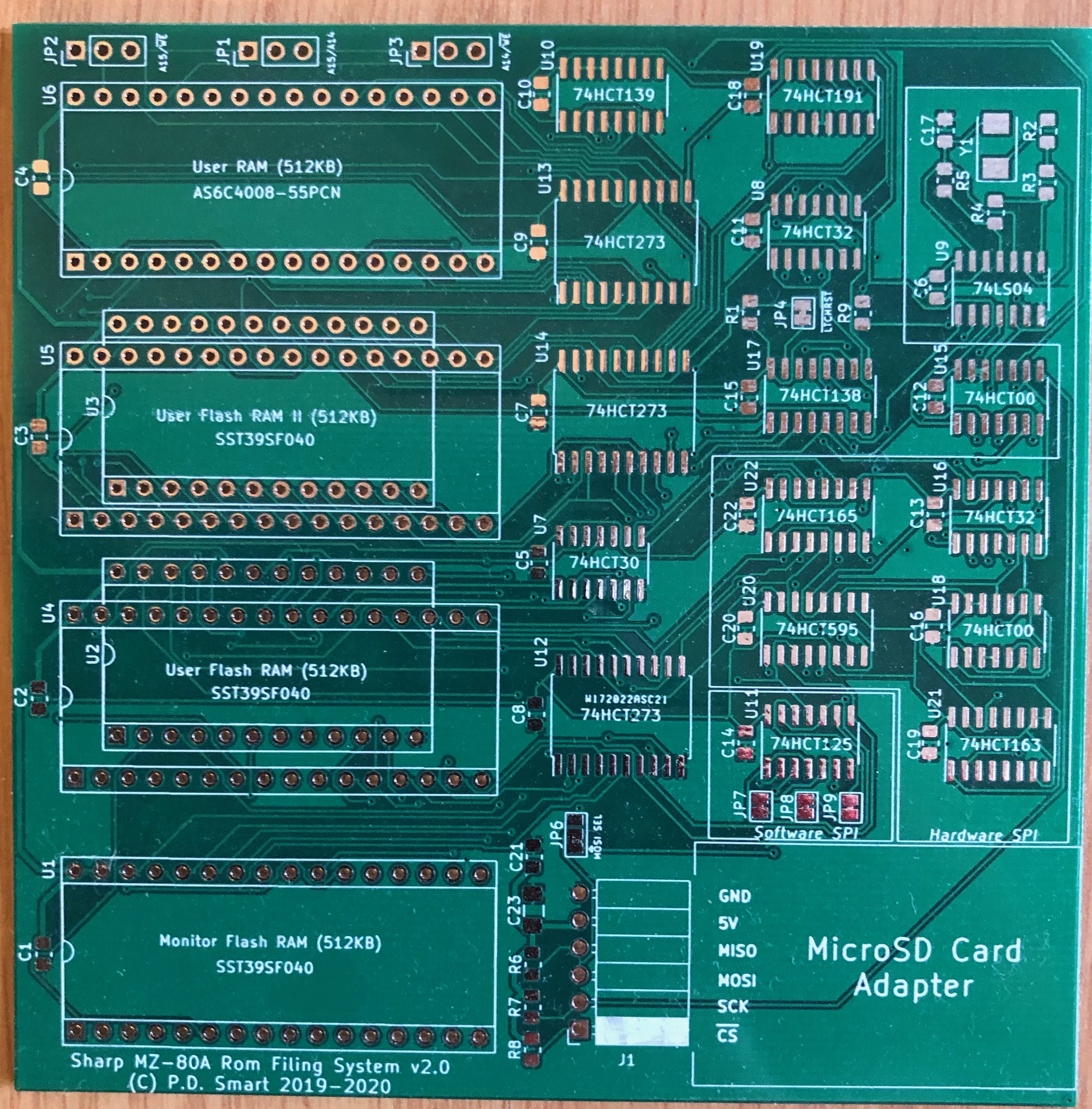
UROMADDR     EQU 0E800H          ; Base of User ROM window
UROMBSTBL    EQU UROMADDR + 020H ; Bank-switch table entry point (0xE820)
RFSJMPTABLE  EQU UROMADDR + 0B0H ; Jump table start (0xE8B0)
FDCROMADDR   EQU 0F000H          ; Floppy AFI ROM address

; Bank control registers (only accessible after coded latch unlock):
BNKCTRLRST   EQU 0EFF8H    ; Read here 16 times to unlock control registers
BNKCTRLDIS   EQU 0EFF9H    ; Read here once to re-lock (disable) control registers
HWSPIDATA    EQU 0EFFBH    ; Hardware SPI data register (read/write)
HWSPISTART   EQU 0EFFCH    ; Hardware SPI start trigger (write to begin transfer)
BNKSELMROM   EQU 0EFFDh    ; Monitor ROM bank select register
BNKSELUSER   EQU 0EFFEh    ; User ROM bank select register
BNKCTRL      EQU 0EFFFH    ; Bank control register (read/write)
Note that BNKCTRLRST through BNKCTRL (0xEFF8–0xEFFF) share the same address space as the top 8 bytes of the Flash ROM window. On reset, these addresses behave as ordinary Flash ROM reads. The coded latch circuit — a 74HCT191 presettable counter — must be unlocked before writes to BNKSELMROM, BNKSELUSER, or BNKCTRL take effect. See the bank-switching section below for the full unlock sequence.
Character and Control Definitions
Standard ASCII control characters are defined as named constants to make the source self-documenting:
BELL    EQU 007H    ; Terminal bell
CR      EQU 00DH    ; Carriage return
LF      EQU 00AH    ; Line feed
CS      EQU 00CH    ; Clear screen (FF)
SPACE   EQU 020H    ; ASCII space
DELETE  EQU 07FH    ; Delete key
Bank Switching in Detail
The RomDisk bank-switching mechanism is fundamentally different from that used by TZFS. TZFS uses the tranZPUter CPLD's memory management modes to remap address ranges in hardware. RomDisk instead uses a physical bank latch — a 74HCT273 D-type flip-flop — accessed through memory-mapped I/O registers at the top of the User ROM address space. Understanding this mechanism is essential before modifying any source file.
Why Banking is Needed
The Sharp MZ-80A gives User ROM only 2 KB of address space (0xE800–0xEFFF). 2 KB can hold only a few hundred instructions — nowhere near enough for a filing system, floppy controller, SD card driver, tape controller, and memory utilities. The solution is to physically switch which 2 KB page of a larger Flash chip is visible at 0xE800–0xEFFF. The RomDisk PCB holds a 512 KB Flash chip divided into 2 KB banks, with up to 12 banks accessible at once. Switching between them on demand gives RFS effectively 24 KB of ROM code while the SA-1510 monitor sees only one static 2 KB window.
The Coded Latch (v2.0 and Later Boards)
The bank select registers share address lines with the top 8 bytes of the Flash ROM (0xEFF8–0xEFFF). If the bank select register were writable at all times, any stray write to that address range — or even Z80 refresh cycles hitting that range — would silently switch banks mid-execution. The RomDisk v2.0 PCB introduced a coded latch to prevent this.
The coded latch is built from a 74HCT191 presettable counter. In its default state (counter not at Terminal Count), the bank control register I/O path is disabled — writes to BNKSELMROM, BNKSELUSER, and BNKCTRL have no effect. To enable the path, software must read from address BNKCTRLRST (0xEFF8) exactly 16 times. Each read increments the counter by one. When the counter reaches Terminal Count (16), it asserts the enable signal that activates the bank control register write path.
After the bank switch is complete, software reads from BNKCTRLDIS (0xEFF9) once. This resets the 74HCT191 to its initial value, deactivating the control register path again. The latch must be re-unlocked before each subsequent bank switch sequence.
The RomDisk v2.1 board added an AND gate (referred to as D1/D2 in the schematic) to prevent the Z80's DRAM refresh cycles from accidentally incrementing the counter. Without this gate, the periodic refresh bus cycles that the Z80 automatically generates could increment the counter on their own, potentially reaching Terminal Count without any deliberate software action and causing spurious bank switches during boot.
The Bank Switch Sequence
A complete bank switch for the User ROM requires the following steps:
Critical: Never Place a Loop Spanning 0xEFF8–0xEFFF
- Unlock the coded latch: Read from address BNKCTRLRST (0xEFF8) exactly 16 times. Each read is a dummy read — the data returned is the Flash ROM byte at that address and can be discarded. Use a loop counter in register B (set to 16), but see the critical warning below about DJNZ placement.
- Write the bank number: Write the desired bank number (0–7 for User ROM banks) to BNKSELUSER (0xEFFE). The 74HCT273 latches the value on the rising edge of the write strobe. For Monitor ROM bank selection, write to BNKSELMROM (0xEFFD) instead.
- Re-lock the latch: Read from BNKCTRLDIS (0xEFF9) once. This resets the 74HCT191 counter and disables the control register write path until the next 16-read sequence.
UROMBSTBL — even if it has never seen bank 3's internal addresses.
This is the most important implementation constraint in the entire RomDisk codebase. The Z80 fetches instruction bytes by reading from the Program Counter address. If any instruction fetch or data read occurs within the range 0xEFF8–0xEFFF, it increments the 74HCT191 counter. A
FusionX Bank Switching (FUSIONX_ENA = 1)
DJNZ instruction at, say, 0xEFF7 will fetch its opcode from 0xEFF7 (no effect), then its offset byte from 0xEFF8 (increments the counter), and on subsequent loop iterations will continue to increment the counter on every pass. If the loop runs 16 or more times before any intentional bank switch, the counter reaches Terminal Count, the control registers become active, and the next write to any address in 0xEFF8–0xEFFF will perform an unintended bank switch — instantly replacing the running code with a different bank.
The rule is simple: no loop instruction (DJNZ, JR, JP) may have its branch target or its own opcode/operand bytes within 0xEFF8–0xEFFF. The GLASS assembler does not automatically detect or warn about this; it is the programmer's responsibility. When adding code to any bank, check that the assembled binary does not place any looping instructions near the top of the 2 KB window.
When
Command Table Format (rfs.asm)
FUSIONX_ENA = 1, the bank-switch stubs include conditional assembly blocks that substitute the FusionX memory management port addresses for the coded latch registers. On a tranZPUter FusionX board, the Flash ROM paging mechanism is replaced by the FusionX CPLD's memory management, which accepts bank numbers via a different I/O port scheme without the 16-read unlock sequence. The RFS command set, SDCFS file system, and all user-visible behaviour remain identical on FusionX — only the low-level bank select writes differ.
The monitor command dispatcher in
rfs.asm uses a compact command table. Each entry describes one command and is laid out as follows:
; One command table entry:
;
;   DB  FLAGS          ; 1 byte: END|MATCH|BANK[5:3]|SIZE[2:0]
;   DB  "COMMAND"      ; SIZE bytes: the command string (no null terminator)
;   DW  HANDLER_ADDR   ; 2 bytes: address of the handler routine in the named bank
;
; Flags byte bit fields:
;   Bit 7 = 1: End of table marker (last entry).
;   Bit 6 = 1: Exact match required (entire input must match; no trailing characters).
;   Bits 5:3   Bank number where HANDLER_ADDR lives (0–7 maps to User ROM banks 0–7).
;   Bits 2:0   Length of the command string in bytes (1–7).
;
; Example — the 'D' (dump) command, handler in bank 3, 1-character string:
    DB  000H | 000H | 018H | 001H    ; not-end, not-exact, bank 3 (011<<3=0x18), length 1
    DB  "D"
    DW  DUMPX
The dispatcher reads the monitor input line, walks the table, and for each entry:
- Compares the first SIZE characters of the input against the command string.
- If the EXACT flag is set, also verifies that no further non-space characters follow.
- If matched, extracts the bank number and handler address from the table entry.
- Performs the bank switch to the target bank via the stub at UROMBSTBL.
- Calls the handler with any remaining input (parameters) available in the monitor input buffer.
LTNX must precede LT, which must precede L, otherwise the shorter entry will match first and the longer command will never be reached.
Module Walkthroughs
rfs.asm — Command Dispatcher (User ROM Bank 0)
Role: The entry point for all RFS functionality. When the SA-1510 monitor does not recognise a command, it passes control to the User ROM entry point at UROMADDR (0xE800). This address is always bank 0.
Key sections:
rfs_bank1.asm — Floppy Disk Controller (User ROM Bank 1)
- ROM entry (ROMFS, 0xE800): A NOP followed by a macro call that selects Monitor ROM bank 0, then a JP to skip over the bank-switch table area. On cold start (detected by checking ROMBK1 for an illegal value ≥ 8), the 16-read coded latch setup sequence is performed and the lower stack area is zeroed. The initial MROM and UROM banks are then selected from saved state in ROMBK1/ROMBK2.
- Bank-switch stub (UROMBSTBL, 0xE820): Sixteen cross-bank call gateways — BKSW0to0 through BKSW0to7 — one for each bank 0→N transition. Each gateway pushes the calling bank number and target bank number onto the stack, then calls the common BKSW0_0 sequence which performs the coded latch unlock, writes the new bank to BNKSELUSER, and jumps to the target handler address. On return (BKSWRET0), the original bank is restored via the same sequence.
- Jump table (RFSJMPTABLE, 0xE8B0): Fixed-address JP instructions for functions that the Monitor ROM or SA-1510 intercept hooks need to call: PRTMZF, PRTDBG, CMT_RDINF, CMT_RDDATA, CMT_WRINF, CMT_WRDATA, CMT_VERIFY, CMT_DIR, CNV_ATOS.
- Command table (CMDTABLE): The RomDisk/picoZ80 build command list. Commands include: drive select (0–9), 40/80 column mode, B (bell toggle), BASIC, C (clear), CP, CPM, D (dump), EC (erase), F (floppy boot), f (AFI ROM), H (help), IR/IC (directory), J (jump), LC/LR/LT and their NX variants (load SD/ROM/tape), M (edit), P (printer test), R (DRAM test), SD2T, SC/ST (save), T (timer test), T2SD, V (verify).
- Initialisation (MONITOR → SIGNON): Checks for tranZPUter board presence via the CPLDINFO I/O port. Sets the initial SD drive number to 0. Detects the active Monitor ROM bank to determine 40-column or 80-column display mode and configures the display accordingly. On video module builds, writes the display mode to the DSPCTL latch.
- Command dispatcher (ST1X): Reads the monitor's input buffer, walks CMDTABLE, extracts bank and handler address on a match, calls the bank-switch stub, and on return loops back to wait for the next command. If no entry matches, returns control to the SA-1510 monitor so it can print its "?" error.
Role: Implements floppy disk boot commands. On the RomDisk build this bank provides the full F (drive-select boot) and f (direct AFI ROM jump) commands.
Key functions:
rfs_bank2.asm — SD Card Controller (User ROM Bank 2)
- FLOPPY (F command): Prompts for a drive number if not supplied on the command line. Writes the drive select and motor enable bytes to I/O port 0xDC (the WD1773 FDC control port). Waits for the spindle motor to reach operating speed (typically 300–500 ms, measured by a CPU cycle-counted delay loop). Reads the boot sector, verifies the bootable-disk signature byte, and passes control to the boot loader code found in the sector.
- FDCK (f command): Reads the byte at FDCROMADDR (0xF000) to verify the AFI ROM is present and non-zero. If found, calls 0xF000 directly, handing control to the original SA-1510 floppy boot ROM. This is useful as a fallback when the WD1773 drive selection logic in FLOPPY is not needed.
Role: The complete SD card subsystem — SPI driver initialisation, SD card command protocol, and the SDCFS directory and file I/O routines. The SPI driver code is selected at assembly time by the HW_SPI_ENA, SW_SPI_ENA, and PP_SPI_ENA flags.
Key functions:
rfs_bank3.asm — Memory Utilities (User ROM Bank 3)
- SDINIT: Implements the SD card SPI initialisation sequence. Deasserts chip select, calls SPIINIT to train the card to the SPI clock, then asserts chip select and sends CMD0 (GO_IDLE_STATE) with up to SD_RETRIES attempts. On success, sends CMD8 (SEND_IF_COND) to detect SD v2 cards, then ACMD41 (SD_SEND_OP_COND) to transition out of idle. Handles SD v1, SD v2, SDHC, SDXC, and MMC v3 cards by checking the OCR response from CMD58.
- SDREAD / SDWRITE: Sector-level read (CMD17, READ_SINGLE_BLOCK) and write (CMD24, WRITE_BLOCK). SDREAD waits for the data start token (0xFE) then reads 512 bytes into the SDBUF RAM buffer. SDWRITE sends the data start token, 512 bytes of data, and a dummy CRC, then waits for the busy signal to clear.
- SDDIR: Reads the directory from the first 8 KB of the active SD drive image into a RAM-resident directory cache. Each directory entry is in MZF header format (128 bytes): file type, filename (17 bytes, Sharp encoding), data size, load address, execution address.
- SDLOAD: Given a file number from the directory cache, calculates the 64 KB-aligned sector address of the file's data block, reads the file's data size bytes, and loads them directly to the Z80 address stored in the directory entry's load address field.
- SDSAVE: Allocates a new directory slot or finds an existing entry with the same name to overwrite. Writes the MZF header fields (start sector, size, load address, exec address), then writes the file data to the corresponding 64 KB block on the SD card.
- SPIINIT: Trains the SD card to the SPI clock. Under HW_SPI_ENA, writes 0xFF to HWSPIDATA and triggers HWSPISTART 10 times (sending 80 '1' bits). Under PP_SPI_ENA (parallel port bit-bang), toggles the clock line 80 times with data held high.
- SPICS: Sets the SD card chip select line. A = 0 activates CS (low), A = 0xFF deactivates CS (high). Under HW_SPI_ENA, modifies the SDCS and BBCLK bits of BNKCTRL and writes back to the hardware register.
- SPIOUT: Sends one byte A to the SD card. Under HW_SPI_ENA: writes A to HWSPIDATA and triggers HWSPISTART — two memory writes, approximately 1 µs per byte at 8 MHz SPI clock. Under PP_SPI_ENA: bit-bangs the byte MSB-first by toggling the clock and data lines on the parallel port, 3 OUT instructions per bit.
- SPIIN: Receives one byte from the SD card. Under HW_SPI_ENA: triggers HWSPISTART to clock in 8 bits, then reads HWSPIDATA. Under PP_SPI_ENA: clocks in each bit by reading the parallel port input register.
Role: Implements the D (hex dump), M (memory edit), and CP (memory copy) commands, available on all builds. The T2SD (tape to SD) and SD2T (SD to tape) commands are also in this bank.
DUMPX (D command): Reads up to 20 lines of 16 bytes each from the target address range. For each line, prints the 4-digit hex address, 16 hex byte values with a space between every 4 bytes, and the 16 corresponding ASCII characters (dot for non-printable bytes). The Sharp MZ uses a proprietary character encoding — bank 6 provides the Sharp-to-ASCII conversion table used here.
MCORX (M command): Interactive memory editor. Presents each byte in sequence showing the address and current hex value. The user types a new 1- or 2-digit hex value and presses Enter to write it, or presses Enter alone to leave the byte unchanged. Ctrl+C or the escape key exits.
MCOPY (CP command): Block memory copy. Accepts source address, destination address, and byte count from the command line as 4-digit hex values. Performs a forward or reverse copy as needed to handle overlapping regions correctly.
T2SD and SD2T: Bidirectional tape↔SD copy. T2SD calls the CMT load routine from bank 4 to read a tape file (including its MZF header) into RAM, then calls the SDSAVE routine from bank 2 to write it to the active SD drive. SD2T calls SDLOAD from bank 2 to load a file to RAM, then calls the CMT save routine from bank 4 to write it to tape. Both commands use the MZF header fields (filename, size, load address, execution address) to keep the directory consistent across media.
rfs_bank4.asm — CMT Controller (User ROM Bank 4)
Role: Implements the LT/LTNX (tape load), ST (tape save), and V (tape verify) commands.
The Sharp MZ-80A uses a 1200 baud Kansas City Standard cassette interface. Bytes are encoded as bursts of 1200 Hz (bit 0) or 2400 Hz (bit 1) tone. The tape routines are time-critical — they must measure the incoming tone frequency and generate the outgoing waveform with microsecond precision. They use the 8253 Programmable Interval Timer (or CPU cycle-counted delay loops on platforms without the timer) to measure bit periods. Interrupts are disabled (
rfs_bank5.asm — Reserved (User ROM Bank 5)
DI) throughout all tape operations to prevent timing disruption.
LOADTAPE / LOADTAPENX: Reads the MZF header from tape (128 bytes: file type, filename, data size, load address, execution address), displays the filename, then reads the data bytes to the load address. LOADTAPE auto-executes by jumping to the execution address after a successful load; LOADTAPENX returns to the RFS command prompt instead.
SAVEX (ST command): Writes the MZF header followed by the data bytes to tape. Accepts start address, end address, and execution address from the command line, or prompts if not provided.
VERIFYX (V command): Reads a tape file and byte-compares it against the RAM at the original load address. Reports any mismatches with their address and expected/actual values.
The MZF header format used by the tape routines is identical to the SDCFS directory entry format. This is not accidental — it is why tape-to-SD copy is completely transparent and why LT-loaded programs can be resaved to SD card with SC without any header conversion.
Role: Currently reserved and unused in the RomDisk build. The bank slot exists in the Flash ROM image and contains the bank-switch stub at the standard offset, but no user-accessible commands are mapped here. This bank is available for future expansion — for example, adding an XModem transfer protocol, a hex loader, or additional memory-mapped hardware drivers.
rfs_bank6.asm — Messages and Character Tables (User ROM Bank 6)
Role: Stores the help screen text, all error and status message strings, and the Sharp MZ character set to ASCII conversion table.
HELPSCR (H command, approximately line 282): A sequence of CR-terminated strings, one per line of the help screen. The BUILD_ROMDISK variant lists all RomDisk commands including T2SD, SD2T, F[X], f, LC, SC, EC, IR/IC, and the drive select digits 0–9. The list is terminated by a single 000H byte. The H command walks this list, printing each string until it encounters the terminator.
PRINTMSG / PRTFN: String printing utilities. PRINTMSG handles embedded marker bytes (e.g. 0xFF to insert a value from the stack) for formatted diagnostic messages. PRTFN prints a Sharp MZ filename (17 bytes in Sharp encoding) as ASCII text using the ATBL conversion table.
ATBL (ASCII-to-Sharp conversion table): A 256-byte lookup table mapping ASCII character codes to their Sharp MZ equivalents and vice versa. The Sharp MZ series uses a proprietary 8-bit character encoding where printable characters have different code points than ASCII — many common characters (letters, digits, punctuation) are shifted or reordered. Any code that displays a filename stored in Sharp encoding on the terminal must pass each byte through this table.
rfs_bank7.asm — Diagnostic Commands (User ROM Bank 7)
Role: Implements the R (DRAM test) and T (timer test) commands on the RomDisk build.
MEMTEST (R command): Performs a walking-bit pattern write/verify test across the full user RAM space (0x1200–0xCFFF). Writes each of the 8 single-bit patterns (0x01, 0x02, 0x04, …, 0x80) to every byte in the range, then reads back and verifies each byte. Any mismatch is reported with its address and the expected/actual values. Run this command after adding any new RAM-resident data structures to verify that addressing is correct before the new structures are used by other code.
TIMERTST (T command): Exercises the 8253 Programmable Interval Timer by programming it into several modes and verifying that it counts and expires as expected. Useful for diagnosing machines where tape operations are unreliable — incorrect 8253 behaviour manifests as systematic timing errors in the CMT bit-rate measurements.
rfs_mrom.asm — Monitor ROM Utilities (Monitor ROM Bank 3)
Role: Provides the ROM scanning and MZF file load routines that must run from Monitor ROM space rather than User ROM space.
Why a separate Monitor ROM bank? The IR and LR commands enumerate MZF program images stored in the upper User ROM Flash banks (User ROM banks above 11 hold packed MZF programs). To scan one of these banks, the firmware must switch the User ROM window to point at that bank. But the scanning code itself lives in User ROM — if it switches the User ROM bank, it instantly replaces its own code with a different bank and crashes.
The solution is to place the scanning loop in Monitor ROM bank 3. Monitor ROM bank switching (via BNKSELMROM) is entirely independent of User ROM bank switching (via BNKSELUSER). Code running in Monitor ROM bank 3 can freely cycle through User ROM banks 12, 13, 14… to enumerate their MZF headers without ever disturbing the Monitor ROM code that is actually executing.
Key functions:
- ROMDIR: Scans all User ROM banks above 11, reads each 128-byte MZF header from the start of each bank, and builds a RAM-resident ROM directory. The directory is used by the IR command to display a list of ROM-resident programs.
- ROMLOAD: Given a file number from the ROM directory, switches the User ROM window to the appropriate bank, reads the MZF header to find the load address and data size, copies the program data from User ROM to the target load address in RAM, and optionally jumps to the execution address. The LRNX variant returns to the RFS command prompt instead of auto-executing.
SPI Driver: Hardware vs Software
The SPI driver in
rfs_bank2.asm is implemented three ways, selected entirely at assembly time. The selection is controlled by the three mutually exclusive flags in rfs_definitions.asm:
HW_SPI_ENA   EQU 1    ; 74HCT595/74HCT165 hardware shift registers on RomDisk v2+ PCB
SW_SPI_ENA   EQU 0    ; Software bit-bang SPI using the RomDisk v2+ I/O port bits
PP_SPI_ENA   EQU 0    ; Software bit-bang SPI via the Sharp MZ-80A parallel printer port
Hardware SPI (HW_SPI_ENA = 1)
Available on RomDisk PCB v2.0 and later. The PCB carries a 74HCT595 serial-out shift register (MOSI/CLK) and a 74HCT165 parallel-in shift register (MISO/CLK) clocked by dedicated hardware logic running at 8 MHz — eight times the Z80's 2 MHz bus clock.
Sending a byte is two memory writes: write the byte to HWSPIDATA (0xEFFB), then write any value to HWSPISTART (0xEFFC). The hardware clocks out all 8 bits automatically in approximately 1 µs. Receiving a byte is similar: write to HWSPISTART to clock in 8 bits, then read HWSPIDATA. The Z80 only needs the time to execute two memory-write instructions between bytes — the hardware shift registers operate concurrently.
Because HWSPIDATA and HWSPISTART live within the 0xEFF8–0xEFFF coded-latch range, they are only accessible while the control registers are unlocked (i.e. after the 16-read sequence). The SDINIT, SDREAD, and SDWRITE routines in bank 2 assume the control registers are already unlocked when they are called, which is always the case within the RFS execution environment.
Software SPI (SW_SPI_ENA = 1)
Available on RomDisk PCB v2.0 and later as a lower-cost alternative to the hardware shift registers. The firmware manually toggles individual bits of the BNKCTRL register (0xEFFF) to drive the SPI clock (BBCLK) and MOSI data (BBMOSI) lines, and reads the MISO bit from BNKCTRL for incoming data. Each bit requires multiple writes to BNKCTRL — toggle clock high, toggle clock low — giving approximately 20–40 µs per byte at 2 MHz Z80 clock speed, roughly 40× slower than hardware SPI.
The SW_SPI_ENA code block in SPIOUT bit-bangs each byte MSB-first using a loop that reads the current BBMOSI and BBCLK state, modifies the relevant bit, and writes back to BNKCTRL. The same coded latch unlock requirement applies — BNKCTRL is only writable after the 16-read sequence.
Parallel Port SPI (PP_SPI_ENA = 1)
The original RomDisk v1 implementation, using the Sharp MZ-80A's Centronics parallel printer port as an improvised SPI bus. The printer port's data lines (D0–D7) are reassigned: one bit drives the SPI clock (CLOCK), one bit drives MOSI data (DOUT), one bit drives chip select (CS), and one bit reads MISO data (DIN) from the port's status register.
Sending a byte in SPIOUT (PP_SPI_ENA path): the byte is rotated left three times to align bit 7 with the DOUT pin position, then an 8-iteration loop drives DOUT and clock high/low using three
Choosing an SPI Variant
OUT (SPI_OUT), A instructions per bit. SPIINIT clocks 80 '1' bits by toggling the clock and data lines 80 times with DJNZ. All parallel port accesses use I/O port instructions (IN / OUT) rather than memory-mapped registers.
PP_SPI_ENA does not require the coded latch unlock — the parallel port lives in the Z80 I/O address space, not the memory address space, so it is always accessible. This was intentional for the v1 design where the coded latch circuit did not yet exist.
| HW_SPI_ENA | SW_SPI_ENA | PP_SPI_ENA | |
|---|---|---|---|
| PCB required | v2.0+ | v2.0+ | v1.x |
| Approx. byte rate | ~1 µs/byte | ~30 µs/byte | ~50 µs/byte |
| Coded latch required | Yes | Yes | No |
| Additional ICs | 74HCT595, 74HCT165 | None | None |
| Suitable for | All current builds | Low-cost v2 variant | Legacy v1 boards |
Adding a New Monitor Command
The following example adds a PEEK command that reads and prints a single byte from a given address. The handler belongs in bank 3 (memory utilities).
Step 1: Write the handler in rfs_bank3.asm
; In rfs_bank3.asm (bank 3, memory utilities):
PEEK:   CALL  HLHEX              ; Parse 4-digit hex address from input buffer into HL
        LD    A,(HL)              ; Read the byte at that address
        CALL  PRTHX              ; Print A as 2 hex digits
        RET
Parameters are available in the monitor input buffer immediately after the command string. HLHEX is a utility routine (available in bank 5 or via the jump table) that reads 4 hex digits from the input buffer and returns the 16-bit value in HL. PRTHX prints the accumulator as two uppercase hex digits.
Step 2: Add a command table entry in rfs.asm
; In rfs.asm, within the CMDTABLE block (inside IF BUILD_ROMDISK+BUILD_PICOZ80 = 1):
;
; Flags byte: not-end (bit7=0), not-exact (bit6=0),
;             bank 3 (bits5:3 = 011 = 0x18), length 4 (bits2:0 = 100 = 0x04)
    DB  000H | 000H | 018H | 004H
    DB  "PEEK"
    DW  PEEK
Place this entry before any shorter entries that share the same leading characters to avoid the shorter entry matching first. The flags byte is constructed as:
000H (not end-of-table) OR 000H (not exact-match) OR 018H (bank 3: 0b011 shifted left 3 = 0x18) OR 004H (command string length 4).
Step 3: Add help text in rfs_bank6.asm
; In rfs_bank6.asm, within the HELPSCR block (before the 000H terminator):
    DB  "PEEKXXXX - read byte at XXXX",    00DH
The help screen uses upper case throughout (lower case characters are difficult to embed in the Sharp character encoding without computing byte values manually).
Step 4: Build
cd /dvlp/Projects/MZ80A_RFS/software/RFS
./build.sh
The assembler will report an error if bank 3 now exceeds 2 KB. If that happens, look for dead code, unused message strings, or duplicate utility routines that can be removed from that bank or moved to bank 5 (currently empty).
Adding New Hardware Support
Adding a New SPI Variant
To add a new SPI hardware variant — for example, a second parallel port design with different bit assignments (PP2_SPI_ENA):
- Add the flag to rfs_definitions.asm:
PP2_SPI_ENA EQU 0 ; Second parallel port SPI variant (custom hardware)
- Add an assertion at the top of rfs_bank2.asm to catch accidental dual-enable:
; Guard: only one SPI flag may be set at a time.
; GLASS does not have a built-in ASSERT directive, so encode this as a build-time
; value check. If more than one flag is set, the total sum exceeds 1 and the error
; manifests as wrong code being assembled into the SPI driver functions.
; (Document this constraint prominently in the comment block above SDINIT.)
- Add conditional assembly blocks in rfs_bank2.asm for each SPI function (SPIINIT, SPICS, SPIOUT, SPIIN). Follow the existing nested IF/ELSE/ENDIF pattern:
SPIOUT:     IF HW_SPI_ENA = 1
              ; Hardware SPI path (existing code)
              LD    (HWSPIDATA),A
              LD    (HWSPISTART),A
              RET
            ELSE
              IF SW_SPI_ENA = 1
                ; Software bit-bang path (existing code)
              ELSE
                IF PP2_SPI_ENA = 1
                  ; New PP2 path:
                  ; (implement bit-bang for the new port layout here)
                  RET
                ELSE
                  ; Original PP_SPI_ENA (centronics) path (existing code)
                ENDIF
              ENDIF
            ENDIF
- Define the new port constants in rfs_definitions.asm alongside the existing SPI_OUT, DOUT_MASK, CLOCK_HIGH etc. constants, guarded with
IF PP2_SPI_ENA = 1 ... ENDIFto avoid symbol conflicts. - Update build.sh if the new variant requires a different Flash image layout or output file name.
To port RFS to a new hardware platform (for example, a new FPGA-based MZ-80A reimplementation):
- Add a BUILD_* flag in rfs_definitions.asm:
BUILD_NEWBOARD EQU 0. - Add address constants if the new board maps ROM windows at different addresses. The most common variation is the User ROM base address and the bank control register addresses.
- Add conditional assembly blocks throughout the source for every point where hardware behaviour differs: bank latch I/O addresses, SPI controller registers, SD card presence detection, display mode switching, and the MONITOR entry-point platform detection code in rfs.asm.
- Add a new bank-switch stub variant in each bank file if the new platform's bank-select mechanism differs from both the coded latch and the FusionX port scheme. The stub at UROMBSTBL must work correctly on cold start before any initialisation has run.
- Update build.sh with a new build section that sets
BUILD_NEWBOARD=1and produces the appropriate ROM image for the new Flash chip layout.
Debugging Tips
Enable debug output: Set
ENADEBUG EQU 1 in rfs_definitions.asm before building. This includes additional diagnostic print statements at strategic points in the SD card initialisation sequence, SDCMD responses, and SDCFS directory parsing. The extra code is conditional and has no effect on the RomDisk ROM image size when disabled.
Dump the User ROM bank 0 entry area: Type D E800 to dump the first 320 bytes of the current User ROM bank. The first few bytes should show the NOP at 0xE800, followed by the HWSELROM macro bytes, followed by a JP instruction. The bank-switch stub at 0xE820 should contain recognisable patterns of PUSH AF / LD A, n sequences. If the dump looks like random data, the coded latch may not have been properly initialised and the wrong bank is being selected.
Check the bank control register: Type D EFF8 to dump the bank control register area. After performing a manual bank switch, the byte at 0xEFFF should reflect the bank number you wrote. If it does not change, check that the 16-read coded latch unlock sequence is being executed before the write.
Verify the coded latch unlock count: If bank control register writes appear to have no effect, the most common cause is that the 16-read sequence is not completing. This can happen if a loop instruction in the bank performs reads from 0xEFF8–0xEFFF during normal execution (see the DJNZ warning in the bank-switching section). Count the read cycles in the unlock sequence and verify the loop counter is set to exactly 16.
v2.1 boot to SA-1510 monitor without + RFS prompt: If the machine boots into the native SA-1510 monitor and the RFS + RFS sign-on line does not appear, the User ROM entry point at 0xE800 is not being called. Check that the coded latch is not being inadvertently triggered by DRAM refresh cycles — the AND gate (D1/D2) on v2.1 was added specifically to prevent refresh cycles from incrementing the 74HCT191 counter. On v2.0 boards without this gate, refresh cycles can reach Terminal Count before the ROM entry point runs.
Run MEMTEST after adding RAM-resident data: Type R immediately after adding new RAM-resident data structures or variables to catch addressing bugs early. A failing address in the 0x1200–0xCFFF range that correlates with the size of a new structure indicates an off-by-one error in the address calculation rather than a faulty RAM chip.
SD card initialisation failures: If SD commands return unexpected response codes with ENADEBUG enabled, verify that the SPI chip select timing is correct — CS must be asserted (low) before CMD0 and maintained throughout the command/response exchange. Under HW_SPI_ENA, check that the SDCS bit in BNKCTRL is being set and cleared correctly by SPICS. Under PP_SPI_ENA, verify that the parallel port output register is initialised before the first SPIINIT call.
Cross-bank call failures: If a cross-bank call appears to execute the wrong code or returns with register corruption, check that the bank-switch stub in the target bank matches the one in bank 0 byte-for-byte. Each bank must have an identical copy of the stub at UROMBSTBL. Use D E820 to dump bank 0's stub, then switch to the target bank manually and dump the same address range to compare.
Reference Sites
| Resource | Link |
|---|---|
| RomDisk hardware page | /sharpmz-upgrades-romdisk/ |
| RFS project page | /sharpmz-upgrades-rfs/ |
| RFS User Manual | /sharpmz-upgrades-rfs-usermanual/ |
| RFS Technical Guide | /sharpmz-upgrades-rfs-technicalguide/ |
| RFS Developer’s Guide (RFS) | /rfs-developersguide/ |
| TZFS Developer’s Guide | /tzfs-developersguide/ |
| tranZPUter FusionX page | /tranzputer-fusionx/ |
| GLASS Z80 Assembler | Bundled in software/RFS/tools/glass.jar |
| Zilog Z80 CPU User Manual | Standard datasheet — bus timing, instruction set, register reference |
| WD1773 FDC Datasheet | Western Digital — floppy disk controller I/O port reference |
| SD Card Physical Layer Spec | SD Association — CMD0/CMD8/ACMD41/CMD17/CMD24 protocol |
| Sharp MZ-80A Service Manual | Hardware schematics, SA-1510 ROM listing, memory map |