 MZ-80A Rom Disk — Technical Guide
RomDisk Technical Guide
This guide documents the Sharp MZ-80A RomDisk PCB hardware design, memory architecture, bank control mechanisms, SPI interface options, software module layout, SD Card Filing System design, CP/M implementation, and the complete build system. It is intended for users who want to understand how the RomDisk works at a system level, build firmware from source, or develop new software that uses the banked ROM environment.
For day-to-day usage and monitor command reference see the RFS User Manual. For Z80 assembly source code walkthroughs see the RFS Developer's Guide.
Hardware Versions
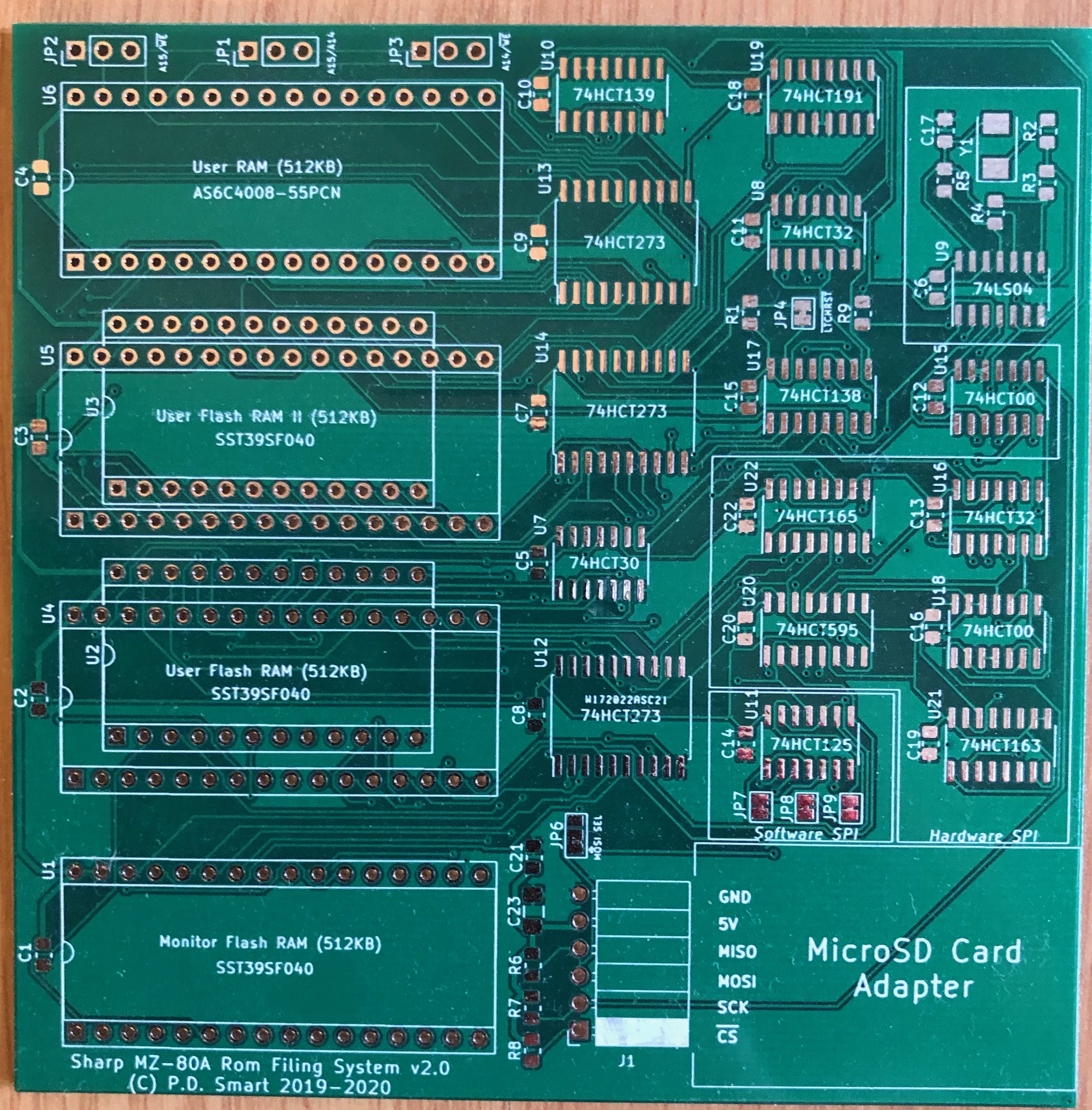
The RomDisk PCB is a daughter card for the Sharp MZ-80A. It plugs into the MZ-80A expansion connector and uses lifter sockets to intercept the Monitor ROM (4 KB at 0x0000–0x0FFF) and User ROM (2 KB at 0xE800–0xEFFF) chip-select lines, replacing both with paged Flash RAM. Three hardware revisions have been produced.
Version 1.1
The original production board. Key features:
Version 2.0
- One 512 KB SST39SF040 Flash RAM in the Monitor ROM socket (U1) — provides eight 4 KB bank slots.
- One 512 KB Flash RAM in the User ROM socket (U4) — provides 256 two-kilobyte bank slots, though RFS uses only the first twelve.
- Simple D-type latch for bank select — the bank register is permanently accessible with no protection mechanism.
- SD card access via software bitbang SPI through the Sharp MZ-80A parallel printer port pins. This method is functional but slow relative to later hardware SPI.
PP_SPI_ENA build flag. There is no coded latch; the bank registers can be written at any time.
A significant revision adding hardware SPI, additional Flash slots, optional SRAM, and a security mechanism for the bank registers:
Version 2.1 (Current)
- Coded latch — a 74HCT191 4-bit up-counter gates the I/O control register decode logic. On power-up, or after a reset read, the counter is at 0 and the bank registers are inaccessible (reads from 0xEFF8–0xEFFF return Flash ROM data as normal). The control registers become active only after exactly 16 sequential reads to the 0xEFF8–0xEFFF range increment the counter to its Terminal Count output. This prevents accidental bank switches when Z80 code happens to access that address region during normal execution.
- Hardware SPI circuit — 74HCT595 serial-to-parallel shift register (MOSI/CLK output) and 74HCT165 parallel-to-serial shift register (MISO input), clocked at 8 MHz from a 16 MHz crystal oscillator. SD card socket fitted directly on the PCB.
- Second and third User ROM Flash slots (U5 and U6) — each a further 512 KB SST39SF040. BK2A19/BK2A20 bits in the BNKCTRL register select which of the three User ROM chips is active.
- Optional 512 KB SRAM — AS6C4008, socketed. Intended for future use as additional paged workspace.
- JP6 solder jumper selects whether the hardware SPI circuit or a software bitbang SPI circuit is fitted.
A targeted bug-fix revision addressing the v2.0 refresh address problem. Changes from v2.0:
- AND gate from discrete diodes (D1/D2) added to the counter clock input. The gate combines the address decode signal with the Z80
/MREQsignal, so only true memory read bus cycles (not refresh cycles) can increment the 74HCT191 counter. Refresh cycles assert/RFSHand deassert/MREQ, so they are blocked. - 0xEFF9 rewired as the dedicated coded latch clear address. A single read to 0xEFF9 resets the 74HCT191 counter to 0 and deactivates I/O control register access.
- PCB silkscreen tidied — component reference designators corrected.
Memory Architecture
The Sharp MZ-80A's Z80 CPU addresses 64 KB of memory. The RomDisk replaces both ROM windows with paged Flash RAM and adds eight I/O control registers in the upper eight bytes of the User ROM address range. The full 0x1200–0xCFFF range remains available for user programs.
Z80 Address Space Layout
Address     Size    Contents
─────────────────────────────────────────────────────────────────────────────
0x0000      4 KB    Monitor ROM window — 4 KB page into 512 KB MROM Flash (U1)
                    Banks: 0 = SA-1510 (40-col, default on power-on)
                           1 = SA-1510 80-column
                           2 = CP/M CBIOS kernel
                           3 = RFS Monitor ROM utilities
                           4 = 1Z-013A MZ-700 monitor
                           5 = 1Z-013A 80-column
                           6 = IPL (Initial Program Loader)
                           7 = (empty)
0x1000      256 B   MZ-80A system variables and stack
0x1200    ~46 KB    User RAM (main program area, 0x1200–0xCFFF)
0xCFFF
0xD000      12 KB   Video RAM + memory-mapped I/O (Sharp MZ-80A mainboard hardware)
0xE800       2 KB   User ROM window — 2 KB page into 512 KB UROM Flash (U4/U5/U6)
                    Banks 0–7:  RFS firmware modules
                    Banks 8–11: CP/M CBIOS modules
0xEFF8       8 B    Coded latch read region (v2+): 16 reads here unlock control registers
                    Also Flash RAM data when latch is closed
0xEFF9       1 B    Coded latch reset: one read re-locks the control registers (v2.1+)
0xEFFB       1 B    HWSPIDATA  — Hardware SPI data register (v2+)
0xEFFC       1 B    HWSPISTART — Hardware SPI start/trigger register (v2+)
0xEFFD       1 B    BNKSELMROM — Monitor ROM bank select register
0xEFFE       1 B    BNKSELUSER — User ROM bank select register
0xEFFF       1 B    BNKCTRL    — Bank control register
0xF000       4 KB   Floppy AFI ROM space (original Sharp floppy controller ROM)
─────────────────────────────────────────────────────────────────────────────
Monitor ROM Banks (4 KB each)
The Monitor ROM window at 0x0000–0x0FFF is bank-switched across eight 4 KB banks stored in the MROM Flash chip at U1. Bank 0 is selected on power-on reset.
| Bank | Module | Description |
|---|---|---|
| 0 | monitor_sa1510.asm |
Original SA-1510 40-column monitor. The default bank on power-on. |
| 1 | monitor_80c_sa1510.asm |
SA-1510 patched for 80-column display (requires Kuma 80-column upgrade). |
| 2 | cbios.asm |
CP/M 2.2 CBIOS kernel — relocated to 0xC000–0xCFFF at runtime during CP/M boot. |
| 3 | rfs_mrom.asm |
RFS Monitor ROM utilities — MZF image scanning and loading. Runs from MROM space so it can page the User ROM without paging itself out. |
| 4 | monitor_1z-013a.asm |
MZ-700 1Z-013A monitor variant. |
| 5 | monitor_80c_1z-013a.asm |
1Z-013A monitor patched for 80-column display. |
| 6 | ipl.asm |
Initial Program Loader. |
| 7 | (empty) | Unused. |
The User ROM window at 0xE800–0xEFFF is bank-switched across 12 active banks spread across the three User ROM Flash chips (U4, U5, U6). The BNKSELUSER register selects the 2 KB page within the active chip; the BK2A19 and BK2A20 bits in BNKCTRL select which chip is addressed.
| Bank | Module | Description |
|---|---|---|
| 0 | rfs.asm |
Primary RFS entry point, command dispatcher, command table, bank-switch infrastructure shared by all banks. |
| 1 | rfs_bank1.asm |
Floppy disk controller (FDC) functions — drive selection and FDC boot. |
| 2 | rfs_bank2.asm |
SD card controller — SPI driver, SD card initialisation, SDCFS directory and file read/write. |
| 3 | rfs_bank3.asm |
Memory utilities — hex dump (D), memory edit (M), memory copy (CP), tape↔SD copy (T2SD/SD2T). |
| 4 | rfs_bank4.asm |
CMT (cassette) controller — tape load, save, and verify. |
| 5 | rfs_bank5.asm |
(Reserved / unused.) |
| 6 | rfs_bank6.asm |
Help screen, message strings, ASCII↔Sharp character set conversion table. |
| 7 | rfs_bank7.asm |
Memory test (R), 8253 timer test (T). |
| 8 | cbios_bank1.asm |
CP/M CBIOS — audio functions and low-level utilities. |
| 9 | cbios_bank2.asm |
CP/M CBIOS — screen driver and ANSI terminal emulation. |
| 10 | cbios_bank3.asm |
CP/M CBIOS — SD card disk driver (CP/M drives A:–G:). |
| 11 | cbios_bank4.asm |
CP/M CBIOS — floppy disk controller. |
Bank Control
Coded Latch Mechanism
On v2.0 and v2.1 boards the bank control registers are protected by a 74HCT191 4-bit up-counter acting as a coded latch. The mechanism prevents Z80 code running from program RAM from accidentally switching ROM banks simply by reading or writing an address that happens to fall in the 0xEFF8–0xEFFF range.
Operation:
Bank Control Register (BNKCTRL, 0xEFFF)
- On power-up or after a latch-reset read, the 74HCT191 counter is at 0. The I/O control register decode logic is disabled — reads from 0xEFF8–0xEFFF return Flash ROM data as normal, and writes to BNKSELMROM/BNKSELUSER/BNKCTRL have no effect.
- To unlock the control registers: perform exactly 16 read cycles to any address in the range 0xEFF8–0xEFFF. Each read increments the counter by one. On v2.1 boards only true memory-read bus cycles (with
/MREQasserted) count; Z80 DRAM refresh cycles (which assert/RFSHand deassert/MREQ) are blocked by the D1/D2 AND gate and do not increment the counter. - When the counter reaches Terminal Count (16), the TC output goes active and enables the I/O control register decode logic. The bank select registers are now writable.
- To re-lock: read from address 0xEFF9 once. This asserts the counter load/reset line, returns the counter to 0, and immediately deactivates the I/O control registers.
The BNKCTRL register controls the SPI bitbang signals, SD card chip select, coded latch configuration, and User ROM chip selection. It is write-only (after the coded latch has been unlocked).
| Bits | Name | Description |
|---|---|---|
| 0 | BBCLK | BitBang SPI Clock output. Toggled by software SPI routines to generate the SPI clock signal. |
| 1 | SDCS | SD Card Chip Select — active low. Set to 0 to select the SD card, 1 to deselect. |
| 2 | BBMOSI | BitBang SPI MOSI data output. Set to the bit value before toggling BBCLK. |
| 5:3 | CDLTCH1–3 | Coded latch configuration bits. Sets the initial counter offset, controlling how many reads to 0xEFF8–0xEFFF are required to unlock the registers. Default 0 = 16 reads required. |
| 6 | BK2A19 | User ROM device/address select bit 0. Combined with BNKSELUSER to address the full 512 KB of each User ROM chip, and to select between U4, U5, and U6. |
| 7 | BK2A20 | User ROM device/address select bit 1. See BK2A19. |
The BK2A19/BK2A20 bits extend the effective User ROM address space beyond the 256 two-kilobyte banks available from BNKSELUSER alone. Together with BNKSELUSER they form a composite address into the three User ROM Flash chips, selecting which chip is active (U4, U5, or U6) and which 2 KB page within it is mapped to the 0xE800–0xEFFF window.
SPI Interface
Three SPI implementations are supported and are selected at build time by setting exactly one flag to
1 in rfs_definitions.asm. Only one may be enabled in a given firmware build.
| Flag | Value | Method | Speed | Hardware Required |
|---|---|---|---|---|
HW_SPI_ENA |
1 | Hardware SPI — 74HCT595/74HCT165 shift registers, 16 MHz crystal | 8 MHz — comparable to Flash ROM access speed | v2.0/v2.1 PCB with JP6 fitted for hardware SPI |
SW_SPI_ENA |
1 | Software bitbang SPI via Z80 I/O port bit manipulation of BNKCTRL | ~300 KB/s — faster than floppy, slower than ROM | v2.0/v2.1 PCB with JP6 fitted for software SPI |
PP_SPI_ENA |
1 | Parallel printer port bitbang (original v1.1 method) | Slowest | v1.1 PCB only |
Hardware SPI operation (v2.0/v2.1 boards):
- Write the data byte to HWSPIDATA (0xEFFB). The 74HCT595 shift register loads the byte ready for transmission.
- Write any value to HWSPISTART (0xEFFC) to begin the transfer. The shift register clocks the byte out on the MOSI line synchronised to the 16 MHz oscillator, while the 74HCT165 simultaneously shifts MISO bits in from the SD card.
- Read HWSPIDATA (0xEFFB) to retrieve the received byte. The complete 8-bit exchange completes in less time than a single Z80 memory read cycle — this is why hardware SPI throughput is comparable to Flash ROM access speed.
Software Architecture
The complete module table — every source file, its target Flash chip, ROM bank, and function:
| Module | Flash Chip | Bank | Size | Description |
|---|---|---|---|---|
rfs.asm |
User (U4) | 0 | 2 KB | Command dispatcher, command table, bank-switch infrastructure. |
rfs_bank1.asm |
User (U4) | 1 | 2 KB | Floppy disk controller — drive select and FDC boot. |
rfs_bank2.asm |
User (U4) | 2 | 2 KB | SD card controller — SPI driver, SDCFS directory, file read/write. |
rfs_bank3.asm |
User (U4) | 3 | 2 KB | Memory utilities — D, M, CP, T2SD, SD2T. |
rfs_bank4.asm |
User (U4) | 4 | 2 KB | CMT controller — tape load, save, verify. |
rfs_bank5.asm |
User (U4) | 5 | 2 KB | (Reserved / unused.) |
rfs_bank6.asm |
User (U4) | 6 | 2 KB | Help screen, message strings, character set conversion. |
rfs_bank7.asm |
User (U4) | 7 | 2 KB | Memory test (R), timer test (T). |
cbios_bank1.asm |
User (U4) | 8 | 2 KB | CP/M CBIOS — audio, low-level utilities. |
cbios_bank2.asm |
User (U4) | 9 | 2 KB | CP/M CBIOS — screen driver, ANSI terminal emulator. |
cbios_bank3.asm |
User (U4) | 10 | 2 KB | CP/M CBIOS — SD card disk driver (drives A:–G:). |
cbios_bank4.asm |
User (U4) | 11 | 2 KB | CP/M CBIOS — floppy disk controller. |
monitor_sa1510.asm |
Monitor (U1) | 0 | 4 KB | Original SA-1510 monitor ROM (40-column). |
monitor_80c_sa1510.asm |
Monitor (U1) | 1 | 4 KB | SA-1510 patched for 80-column display. |
cbios.asm |
Monitor (U1) | 2 | 4 KB | CP/M 2.2 CBIOS kernel (relocated to 0xC000 during CP/M boot). |
rfs_mrom.asm |
Monitor (U1) | 3 | 4 KB | RFS Monitor ROM utilities — ROM scanning, MZF loading. |
monitor_1z-013a.asm |
Monitor (U1) | 4 | 4 KB | MZ-700 1Z-013A monitor variant. |
monitor_80c_1z-013a.asm |
Monitor (U1) | 5 | 4 KB | 1Z-013A patched for 80-column display. |
ipl.asm |
Monitor (U1) | 6 | 4 KB | Initial Program Loader. |
Because the Z80 can only see a 2 KB slice of User ROM at any one time, every User ROM bank contains a copy of the bank-switching stub at a fixed address within the window. When bank 0 needs to call a routine in bank 3, it writes the destination bank number to BNKSELUSER, jumps to the well-known entry point in the newly mapped bank, executes the required code, writes bank 0 back to BNKSELUSER, and returns. This mechanism makes all 12 × 2 KB = 24 KB of User ROM code accessible from any execution context.
Important constraint on v2.0/v2.1 boards: no tight loop instruction sequence in User ROM bank code may span the address range 0xEFF8–0xEFFF, as repeated reads to that range will increment the coded latch counter and eventually unlock the bank registers unexpectedly.
SD Card Filing System (SDCFS)
Rather than implementing FAT (which would be too large to fit within the available 2 KB ROM banks), the RomDisk firmware uses a purpose-built filing system called the SD Card Filing System (SDCFS). The design prioritises simplicity and a minimal ROM footprint over flexibility.
The SD card is used raw — no partition table is written. The SDCFS image begins at byte 0 (sector 0) of the card. CP/M disk images are placed at the 256 MB boundary to ensure all 10 RFS drives have room regardless of how full they become.
Directory Structure
Each SDCFS drive contains a flat directory of up to 256 entries. Each entry is exactly 32 bytes, using a structure derived from the standard MZF tape header format (the same 32-byte layout used on Sharp MZ cassette tapes):
| Field | Bytes | Description |
|---|---|---|
| FLAG1 | 1 | Bit 7 = 1: valid entry. Bit 7 = 0: inactive / deleted. |
| FLAG2 | 1 | MZF execution type (0x01 = binary program). |
| FILE NAME | 17 | Standard 17-character MZF filename (Sharp character encoding). |
| START SECTOR | 4 | First SD card sector within this drive image where the file’s data block begins. |
| SIZE | 2 | Actual byte count of the file data. |
| LOAD ADDR | 2 | Z80 RAM address to load the file data to. |
| EXEC ADDR | 2 | Auto-execution address for binary files (jumped to after load if non-zero). |
| RESERVED | 3 | Not currently used. |
The directory occupies the first 8 KB of each drive image (256 entries × 32 bytes). File data immediately follows. Each file is allocated a fixed 64 KB block — matching the maximum Sharp MZ cassette tape block size — which keeps the on-disk layout trivially simple and makes SD↔tape copy a direct sector-aligned byte-for-byte transfer.
SD Card Layout
ADDRESS       CONTENT
────────────────────────────────────────────────────────────────────────
0x00000000    RFS DRIVE 0  (16 MB)
                0x00000000–0x00001FE0  Directory (256 × 32 B)
                0x00002000–0xFF2000    File blocks (256 × 64 KB)
0x01002000    RFS DRIVE 1  (same structure)
...
0x09012000    RFS DRIVE 9  (same structure)
0x0A014000    (padding to 256 MB boundary)
────────────────────────────────────────────────────────────────────────
0x10000000    CP/M DISK IMAGE 0  (A:)  — 16 MB
0x11000000    CP/M DISK IMAGE 1  (B:)  — 16 MB
...
0x16000000    CP/M DISK IMAGE 6  (G:)  — 16 MB
────────────────────────────────────────────────────────────────────────
CP/M 2.2 Implementation
CP/M 2.2 is available on the RomDisk as a built-in capability. Entering
Boot Process
CPM at the RFS monitor prompt boots CP/M directly from the SD card. The CP/M TPA is 47 KB; the CCP sits at 0x9C00 with BDOS above it, while the entire CBIOS lives in ROM (Monitor ROM bank 2 plus User ROM banks 8–11) and consumes no program RAM.
- The RFS
CPMcommand switches the Monitor ROM to bank 2 (the CBIOS kernel), which contains the CP/M cold-boot entry point at 0x0000. - The CBIOS cold-boot routine initialises all hardware (keyboard, screen, SD card, floppy if present) and builds the Disk Parameter Headers for each available drive.
- The CBIOS reads the CCP and BDOS images from the CP/M system disk on the SD card into RAM at 0x9C00.
- Control passes to the CCP at 0x9C00. CP/M is now running.
The Custom BIOS is split across five ROM modules so that no single 2 KB bank is exceeded:
| Module | ROM Location | Contents |
|---|---|---|
cbios.asm |
Monitor ROM bank 2 (0x0000–0x0FFF while active) | All 17 CP/M CBIOS API vectors, cold/warm boot handlers, interrupt handler, disk parameter tables. |
cbios_bank1.asm |
User ROM bank 8 | Audio (bell, melody), real-time clock routines, low-level keyboard handler. |
cbios_bank2.asm |
User ROM bank 9 | Screen driver (character output, scroll, cursor control), ANSI/VT100 terminal emulator. |
cbios_bank3.asm |
User ROM bank 10 | SD card disk driver — translates CP/M 128-byte sector reads and writes to SDCFS drive images at the 256 MB boundary. |
cbios_bank4.asm |
User ROM bank 11 | Floppy disk controller — supports physical CP/M floppy disks. |
CP/M drives are mapped to SD card disk images during the CBIOS cold-boot. The standard drive mapping is:
| CP/M Drive | Image | Contents |
|---|---|---|
| A: | CP/M Disk Image 0 | OS programs, Turbo Pascal, Hi-Soft C, Fortran 80, MS-BASIC 80. |
| B: | CP/M Disk Image 1 | Pascal MTP v5.61, Turbo Pascal v3.00a, Pascal User Group disks. |
| C: | CP/M Disk Image 2 | PLI, PLM 80, WordStar v3.0/v3.3/v4.0. |
| D:–G: | CP/M Disk Images 3–6 | Grant Searle CP/M collection disks. |
Build System
All development is done under Linux (Debian/Ubuntu). The build system is self-contained within the repository. The top-level entry point is
Prerequisites
build.sh in the software/RFS/ directory.
| Tool | Purpose |
|---|---|
| Java JRE 8+ | Runs the GLASS Z80 assembler (tools/glass.jar). java must be on PATH. |
| bash | All build scripts are bash shell scripts. |
| perl | Required by tools/mzftool.pl for MZF file manipulation. |
| gcc / make | Compiles cpmtools from source on first build (automatic). |
| dd, cat, stat | Standard Linux utilities used by the packaging scripts. |
The GLASS Z80 assembler is bundled as
Build Flags
tools/glass.jar — no separate installation is required.
Edit
asm/include/rfs_definitions.asm before building. The SPI interface flags are mutually exclusive — set exactly one to 1:
| Flag | Default | Description |
|---|---|---|
HW_SPI_ENA |
1 | Hardware SPI (v2.0/v2.1 PCB, JP6 configured for hardware SPI). Default for all current boards. |
SW_SPI_ENA |
0 | Software bitbang SPI (v2.0/v2.1 PCB, JP6 configured for software SPI). |
PP_SPI_ENA |
0 | Parallel port bitbang SPI. For v1.1 boards only. |
FUSIONX_ENA |
1 | Include tranZPUter FusionX support. |
ENADEBUG |
0 | Enable assembly-time debug output. |
git clone https://github.com/pdsmart/RFS.git
cd RFS/software/RFS

# Full build — assembles all ROMs, packages Flash images, builds SD card image:
./build.sh

# Full build including reprocessing all MZF application files
# (only needed when files in MZF/ have changed):
./build.sh -m
build.sh runs the following steps in order:
- Compiles
cpmtoolsfrom source if not already built, and adds it toPATH. tools/assemble_rfs.sh— assembles all RFS firmware banks (rfs.asm, rfs_bank1–7.asm) into individual ROM images.tools/assemble_cpm.sh— assembles the CP/M 2.2 CBIOS (cbios.asm, cbios_bank1–4.asm) and the CP/M CCP+BDOS kernel.tools/assemble_roms.sh— assembles all monitor variants (SA-1510, 80c, 1Z-013A, IPL) and MZF application binaries.tools/processMZFfiles.sh(only with-mflag) — converts raw MZF files fromMZF/into 128-byte and 256-byte sector-padded images inMZB/.tools/make_roms.sh— packages assembled ROM images and MZF application binaries into 512 KB Flash ROM images for each Flash chip.tools/make_cpmdisks.sh— creates CP/M disk images in RAW format (for SD card) and CPC Extended Disk Format (for floppy emulators).tools/make_sdcard.sh— combines the 10 RFS drive images and 7 CP/M disk images into the final SD card image.
After a successful build the
roms/ directory contains:
| File | Target Chip | Description |
|---|---|---|
MROM_ROMDISK_256.bin |
Monitor ROM Flash (U1) | Monitor ROM image: SA-1510, 80c SA-1510, CP/M CBIOS, RFS mrom utils, 1Z-013A monitors, IPL across 7 × 4 KB banks. |
USER_ROM_256.bin |
User ROM Flash U4 | RFS banks 0–7, CP/M CBIOS banks 8–11, packed MZF applications. |
USER_ROM_II_256.bin |
User ROM Flash U5 | Additional MZF applications (overflow from U4). |
USER_ROM_III_256.bin |
User ROM Flash U6 | Additional MZF applications (overflow from U5). |
SHARP_MZ80A_RFS_IMAGE_0–9.img |
SD card | Individual RFS drive images, one per drive (drives 0–9). |
SHARP_MZ80A_RFS_CPM_IMAGE_1.img |
SD card | Combined image: 10 RFS drives + 7 CP/M disk images. Write this file to the SD card. |
To program the Flash chips, use a suitable SST39SF040-compatible programmer. Write
MROM_ROMDISK_256.bin to U1, USER_ROM_256.bin to U4, and the overflow images to U5 and U6 if fitted. To write the SD card image use dd:
dd if=roms/SHARP_MZ80A_RFS_CPM_IMAGE_1.img of=/dev/sdX bs=512 status=progress
Reference Sites
| Resource | Link |
|---|---|
| RomDisk project page | /sharpmz-upgrades-romdisk/ |
| RFS project page | /sharpmz-upgrades-rfs/ |
| RFS User Manual | /sharpmz-upgrades-rfs-usermanual/ |
| RFS Developer’s Guide | /sharpmz-upgrades-rfs-developersguide/ |
| RFS Technical Guide | /sharpmz-upgrades-rfs-technicalguide/ |
| RFS Gallery | /sharpmz-upgrades-rfs-gallery/ |
| SFD-700 mkII Technical Guide | /sfd700-technicalguide/ |
| picoZ80 Technical Guide | /picoz80-technicalguide/ |
| GLASS Z80 Assembler | Bundled in tools/glass.jar |
| SST39SF040 Flash datasheet | Microchip / Greenliant product page |
| AS6C4008 SRAM datasheet | Alliance Memory product page |