 SFD-700 mkII Technical Guide
SFD-700 mkII Technical Guide
This guide documents the SFD-700 mkII hardware architecture, CPLD functional blocks, I/O register map, memory map, and build and programming procedures. It is intended for users who want to understand how the card works, troubleshoot at a hardware level, modify the firmware, or build the card from the supplied source files.
For end-user setup and installation see the User Manual. For VHDL source code walkthroughs and firmware development see the Developer's Guide.
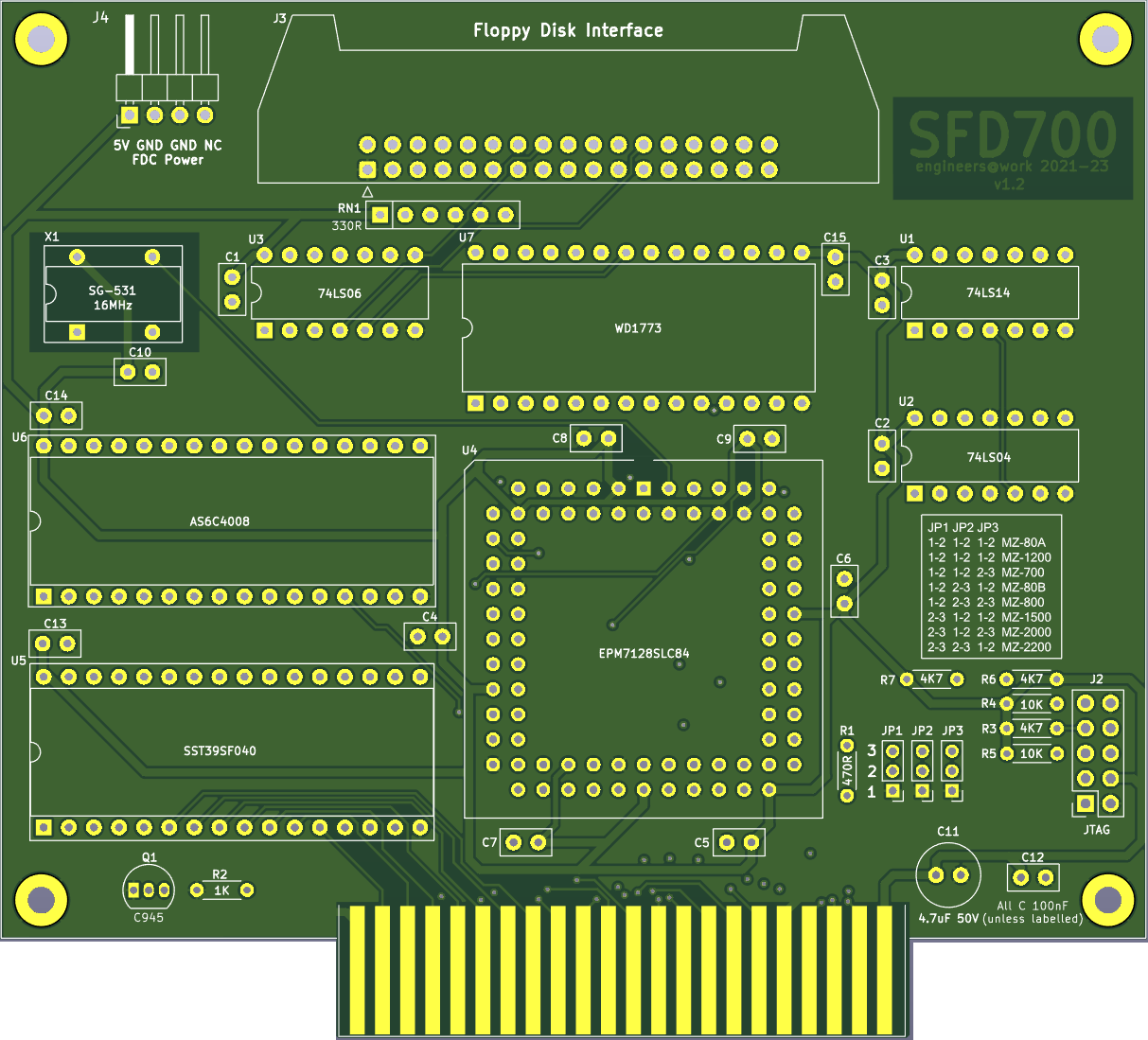
System Architecture
The SFD-700 mkII is a bus-connected expansion card. It sits on the Z80 address, data, and control bus of the host Sharp MZ computer and presents itself as a set of memory-mapped and I/O-mapped resources. The central intelligence is a CPLD that decodes every bus cycle and routes signals appropriately.
System Block Diagram
┌──────────────────────────────────────────────────────────────────┐
│                    SFD-700 mkII v1.2 PCB                         │
│                                                                  │
│  Host Z80 Bus (A[15:0], D[7:0], MREQ, IORQ, RD, WR, RESET)     │
│  ────────────────────────────┬───────────────────────────────    │
│                              │                                   │
│              ┌───────────────┴───────────────┐                  │
│              │     EPM7128SLC84-15 CPLD       │                  │
│              │                               │                  │
│              │  • I/O address decode          │                  │
│              │  • Memory address decode       ├──► ROM_CSn       │
│              │  • ROM/RAM page registers      ├──► RAM_CSn       │
│              │  • MZ-700/1500 mem mgmt        ├──► ROM_A10       │
│              │  • Drive/motor/side/dden regs  ├──► RAM_A10       │
│              │  • Data bus inversion (ID bus) ├──► FDCn          │
│              │  • Clock divide (16→8 MHz)     ├──► CLK_FDC       │
│              │  • Interrupt gating            ├──► DRVSAn/Bn/Cn/Dn│
│              │  • Mode latch (from jumper)    ├──► MOTOR / SIDE1 │
│              └──────────────┬────────────────┘   DDENn          │
│                             │                                    │
│            ┌────────────────┼────────────────┐                  │
│            │                │                │                  │
│     ┌──────┴──────┐  ┌──────┴──────┐  ┌──────┴──────┐          │
│     │  WD1773 FDC │  │ Flash ROM   │  │  SRAM       │          │
│     │  (inverted  │  │ 512KB       │  │  32KB       │          │
│     │   data bus) │  │ (AFI + RFS) │  │ (workspace) │          │
│     └──────┬──────┘  └─────────────┘  └─────────────┘          │
│            │                                                     │
│     ┌──────┴──────────────────────────┐                         │
│     │    34-pin floppy connector J3   │                         │
│     │  (DRVSAn-Dn, MOTOR, SIDE, DDEN,│                         │
│     │   STEP, DIR, WGATE, DATA lines) │                         │
│     └──────────────────────────────── ┘                         │
│                  │                                               │
│           Floppy Drives A–D                                      │
└──────────────────────────────────────────────────────────────────┘
PCB Revision History
The SFD-700 mkII has gone through three hardware revisions. The fundamental circuit topology is the same across all revisions; the differences are primarily in the programmable logic implementation.
| Version | Programmable Logic | Status | Notes |
|---|---|---|---|
| v1.0 | Two Lattice GALs (GAL26CV12 + GAL16V8) | Reference only — do not build | Functional on MZ-700 inside MZ-1U06. GAL register count limits prevented full memory management + ROM paging simultaneously. |
| v1.1 | Two Lattice GALs (GAL26CV12 + GAL16V8) | Reference only — do not build | Minor PCB corrections. Same GAL limitations as v1.0. |
| v1.2 | Single Altera EPM7128SLC84-15 CPLD | Current — recommended | Replaces both GALs. Full MZ-700/MZ-1500 memory management and independent ROM/RAM paging. Tested on MZ-80A, MZ-700, MZ-1500, MZ-2000. |
Key Integrated Circuits
EPM7128SLC84-15 — CPLD (v1.2)
The Altera MAX7000S EPM7128SLC84-15 is an EEPROM-based Complex Programmable Logic Device in an 84-pin PLCC package. Key characteristics:
WD1773 — Floppy Disk Controller
- 128 macrocells — each macrocell is a programmable sum-of-products logic cell with a D-type flip-flop register. 72 of the 128 are used by this design.
- 15 ns maximum propagation delay — fast enough to decode bus cycles and respond within the Z80's setup/hold windows.
- 5V tolerant inputs — the MAX7000S family can accept 5V signals directly from the Sharp MZ bus, making level conversion unnecessary.
- EEPROM configuration storage — the programmed logic is retained in on-chip EEPROM indefinitely. No external configuration memory or boot delay.
- In-system programmable via JTAG — the CPLD can be reprogrammed without removing it from the board, using the 10-pin JTAG header and a USB-Blaster.
- 68 user I/O pins — 65 of 68 available I/O pins are used (96% utilisation).
The Western Digital WD1773 is a single-chip Floppy Disk Controller that implements the full read/write data separation, track formatting, and sector access logic in hardware. It is a direct descendant of the WD1771/WD1772 family and is bus-compatible with the WD179x series.
Key WD1773 characteristics relevant to this design:
SST39SF040 (or compatible) — 512 KB Flash ROM
- Inverted data bus — the WD1773 requires all 8 data bus bits to be inverted (logic high becomes logic low and vice versa). The CPLD handles this transparently using a dedicated inverted data bus (ID[7:0]).
- DRQ (Data Request) — the WD1773 asserts DRQ when it has a byte ready to be read (or needs a byte written) during a data transfer. On the MZ-80A (MODE 0) the CPLD routes DRQ to Flash ROM address bit A10 so that the 2 MHz CPU can service transfers by executing different ROM code paths rather than polling.
- INTRQ (Interrupt Request) — asserted when a command completes. The CPLD gates this signal through a software-controlled enable bit, routing it to the Z80's INT line only when enabled by writing to port 0xDF.
- 8 MHz clock required — the WD1773 needs an 8 MHz input clock for standard MFM (double density) operation. The CPLD generates this by dividing the 16 MHz crystal oscillator by two.
The Flash ROM stores the machine boot firmware (AFI ROM) and the ROM Filing System. It is organised as 128 × 4 KB pages, addressable through the CPLD's two paged memory windows (EXXX and FXXX). The CPLD drives the upper address bits (A10 and above via the ID bus) to select the active page. The device is programmed in-circuit or externally using a standard Flash programmer.
Clock Architecture
A 16 MHz crystal oscillator (X1) provides the primary clock. This drives the CPLD's dedicated global clock input (
CLK_16M). Inside the CPLD, a single toggle flip-flop (the FDCCLK process) divides this by two, producing an 8 MHz clock (CLK_8Mi) which is output on pin CLK_FDC directly to the WD1773 chip-clock pin.
All registered processes in the CPLD (the page registers, drive registers, interrupt enable, and memory management state) are clocked by the 16 MHz clock — this gives a 62.5 ns clock period, well within the setup-and-hold requirements of the Z80 bus cycles on all supported host machines (the slowest, the MZ-80A, runs at 2 MHz = 500 ns clock period).
The host Z80 clock (CLK_BUS0) is connected to a CPLD input pin but is not used in the current logic — bus cycle decoding is entirely combinatorial (address and control signals decoded asynchronously). The pin is reserved for future use.
I/O Address Decoding
The CPLD monitors the Z80's IORQn, RDn, WRn, and A[7:0] lines and generates internal select signals whenever an I/O bus cycle falls within a recognised port address. All decoding is purely combinatorial — results are available within one CPLD propagation delay (15 ns maximum) of the bus signals becoming valid.
Three address blocks are decoded:
- 0xD8–0xDB — WD1773 FDC registers (Status/Command, Track, Sector, Data). The CPLD asserts FDCn (WD1773 chip select) for both reads and writes, and simultaneously controls the ID data bus direction for the data inversion.
- 0xDC–0xDF — FDC control registers (drive/motor, head side, data density, interrupt enable). These are write-only registers (except 0xDF which is also read to disable interrupts) implemented as flip-flops inside the CPLD.
- 0x60–0x63 — ROM/RAM paging registers (EXXX page, FXXX page, ROM/RAM select, MODE readback). These are readable and writable.
- 0xE0–0xE6 — host memory management ports. Writes are intercepted by the CPLD to track the host's paging state and suppress the SFD-700's own ROM/RAM chip selects as appropriate.
Memory Address Decoding
The CPLD also monitors Z80 memory cycles (MREQn asserted with RDn or WRn) and generates chip-select outputs for the Flash ROM and SRAM:
- EXXX window (E300h–EFFFh) — selected when MREQn is low and the Z80 address is in the range 0xE3xx–0xEFxx. The lower boundary is 0xE300 rather than 0xE000 because E000h–E2FFh is reserved for MZ-700/MZ-1500 memory-mapped I/O and must not be occupied by the expansion card.
- FXXX window (F000h–FFFFh) — selected when MREQn is low and the Z80 address is in the range 0xF0xx–0xFFxx.
Data Bus Inversion
The WD1773 uses a historical convention where all data bus bits are inverted: a logic '1' on the Z80 data bus appears as logic '0' on the WD1773 data bus and vice versa. Rather than using discrete inverter ICs (which would add component count and propagation delay), the CPLD handles this inline.
The CPLD connects to two bidirectional 8-bit buses:
- Z80_DATA[7:0] — the host Z80 data bus (non-inverted).
- ID[7:0] — the inverted data bus, connected to the WD1773 data pins and also used as the upper address bits to the Flash ROM and SRAM.
- Z80 read from FDC (0xD8–0xDB): The WD1773 drives ID[7:0] with inverted data. The CPLD reads ID and re-inverts it before driving Z80_DATA, so the host sees correct (non-inverted) data.
- Z80 write to FDC (0xD8–0xDB): The CPLD takes Z80_DATA, inverts every bit, and drives the result onto ID[7:0] so the WD1773 receives the expected inverted representation.
- Memory accesses (EXXX/FXXX windows): When a memory chip select is active, the ID bus doubles as the upper address lines to the Flash ROM and SRAM. The CPLD drives ID[7:0] with {page_register[6:0], Z80_ADDR[11]} — providing 7 page bits and the natural A11 line to the storage device.
ROM / RAM Paging
The SFD-700 mkII maps 4 KB pages of the 512 KB Flash ROM or 32 KB SRAM into two windows in the Z80 address space. Both windows are independently controlled by software-writable page registers inside the CPLD.
| Window | Address Range | Page Register (I/O port) | Page width | Max storage |
|---|---|---|---|---|
| EXXX | E300h–EFFFh | 0x60 (bits [6:0]) | 4 KB | 128 × 4 KB = 512 KB |
| FXXX | F000h–FFFFh | 0x61 (bits [6:0]) | 4 KB | 128 × 4 KB = 512 KB |
I/O port 0x62 selects whether the Flash ROM or SRAM is active (D0 = 0 → Flash ROM; D0 = 1 → SRAM). Both windows are switched together by this register.
On reset:
- The EXXX page register is initialised to page 2 (decimal) — "Customised UROM containing RFS start bank".
- The FXXX page register is initialised to page 0 for MZ-80A/MZ-1200 (AFI ROM for MZ-80A), or page 1 for MZ-700 (AFI ROM for MZ-700).
- The RAMEN register is cleared — Flash ROM is active by default.
MZ-700 / MZ-1500 Memory Management
The MZ-700 and MZ-1500 include a hardware memory management controller that banks the internal 64 KB DRAM and the character generator ROM in and out of the upper address space. This affects addresses D000h–FFFFh — exactly the range used by the SFD-700 mkII's ROM and RAM windows.
The host operating system controls the mapping by writing to I/O ports 0xE0–0xE6. The CPLD monitors these writes and maintains two internal state flags:
| Port | Action | Effect on SFD-700 mkII |
|---|---|---|
| 0xE1 | Host maps DRAM to D000h–FFFFh | Sets REG_ROMDIS — SFD-700 ROM/RAM is disabled |
| 0xE3 | Host maps memory-mapped I/O to D000h | Clears REG_ROMDIS — SFD-700 ROM/RAM re-enabled |
| 0xE4 | Host maps monitor ROM + DRAM | Clears REG_ROMDIS — SFD-700 ROM/RAM re-enabled |
| 0xE5 | Host inhibits all D000h–FFFFh access | Sets REG_ROMINH — SFD-700 ROM/RAM is disabled |
| 0xE6 | Return to default mapping | Clears REG_ROMINH — SFD-700 ROM/RAM re-enabled |
REG_ROMINH takes priority over REG_ROMDIS. When REG_ROMINH is set, the SFD-700 mkII's chip selects are suppressed regardless of the REG_ROMDIS state. Both flags are cleared by a Z80 RESET.
This design allows the SFD-700 mkII to coexist correctly with all MZ-700 and MZ-1500 software that performs memory management operations, including CP/M, BASIC, and the operating system itself — no special software driver is required on the host side.
MZ-80A DRQ-to-Address-Line Trick
The Sharp MZ-80A (and MZ-1200) runs its Z80 CPU at 2 MHz. A floppy disk in standard MFM double-density mode produces a new data byte from the WD1773 every 32 µs. At 2 MHz, the Z80 can execute approximately 16 instructions in 32 µs — which is sufficient for a polling loop in fast RAM, but the original K&P SFD-700 stored its boot code in ROM, and the additional ROM access overhead reduced the effective instruction rate below what was needed to reliably drain the WD1773's data register before overrun.
Sharp's solution (adopted here) is to connect the WD1773 DRQ output to Flash ROM address bit A10. This works as follows:
- The boot ROM contains two copies of the sector-read routine in alternate 1 KB segments. Both copies are functionally identical except that one immediately reads the WD1773 data register (taken when DRQ = 1, meaning data is ready), and the other loops back to wait (taken when DRQ = 0, meaning data is not yet ready).
- DRQ is high when a byte is available. With DRQ wired to A10, the CPU naturally executes the "read data" path of the ROM when data is ready, and the "wait" path when it is not — no polling instruction is needed, and the CPU wastes zero cycles checking a flag.
- The CPLD implements this in MODE 0 only:
ROM_A10 ≤ '1' when (MODE = MZ-80A) and DRQ = '1', else Z80_ADDR(10). For all other modes, ROM_A10 follows the natural Z80 address bit 10.
Interrupt Control
The WD1773 asserts INTRQ when a command completes (type I, II, and III commands) and when a Force Interrupt command (type IV) is issued. The CPLD gates this signal through a registered enable bit (REG_INT):
- Write to 0xDF: sets REG_INT = 1 — INTRQ is now routed to the Z80 INT line.
- Read from 0xDF: clears REG_INT = 0 — the Z80 INT line is deasserted.
- RESET: REG_INT is cleared asynchronously.
GAL Logic (v1.0 / v1.1)
Versions 1.0 and 1.1 of the SFD-700 mkII used two Lattice GAL devices instead of the CPLD. These are documented here for completeness and for those who have a v1.0 or v1.1 board.
GAL26CV12 (U1, GAL1) — I/O Decoder and Memory Management
The primary logic device. It decoded the Z80 I/O address bus for all FDC accesses, generated the bus buffer direction signal, tracked MZ-700 memory paging state using its registered outputs, and controlled the interrupt enable flag. Its main limitation was that the single registered output cluster could not simultaneously hold the full MZ-700 memory management state and the ROM paging registers — these were implemented as external discrete flip-flops driven by strobes from the GAL, rather than as internal state. GAL16V8 (U2, GAL2) — ROM Decoder
Handled memory-side address decoding, generating the ROM chip select for the F000h–FFFFh window, multiplexing the DRQ signal onto Flash ROM address bit A10 (for MZ-80A), and selecting the firmware page via the MODESEL jumper. Building the GAL files
The CUPL source files are in the
CUPL/ directory. Compilation requires Logical Devices CUPL v4.0 (DOS-era) because WinCUPL does not support the Lattice GAL26CV12. Run under DOSBox:
cupl -j -f -a g26cv12 SFD700_1    # Compile GAL1 (GAL26CV12)
cupl -j -f -a g16v8  SFD700_2    # Compile GAL2 (GAL16V8)
Programming the GALs
The GAL16V8 (GAL2) is directly supported by all modern programmers including the TL-866 II+:
The GAL16V8 (GAL2) is directly supported by all modern programmers including the TL-866 II+:
minipro -p GAL16V8 -w SFD700_2.JED
The GAL26CV12 (GAL1) requires a PLCC-28 to DIP-28 adapter and a custom
infoic.xml device database entry (provided in the CUPL/ directory):
minipro -p GAL26CV12 -w SFD700_1.JED
CPLD Architecture (v1.2)
The v1.2 CPLD design uses 72 of 128 available macrocells (56%), with 37 registers and 65 I/O pins. Both global clock resources are used: CLK_16M for all registered processes, and Z80_RESETn for synchronous/asynchronous reset. The 72 macrocells are logically partitioned into the following functional blocks:
| Block | Macrocells | Description |
|---|---|---|
| Clock divider | 1 | Toggle flip-flop: 16 MHz → 8 MHz for WD1773 |
| I/O address decoder | ~15 | Combinatorial decode of all I/O port select signals |
| Memory address decoder | ~4 | Combinatorial decode of EXXX and FXXX window selects |
| Mode register | 3 | 3-bit registered latch of MODE jumper, sampled on RESET |
| Drive/motor register | 5 | 4 drive-select bits + motor enable bit (port 0xDC) |
| Side register | 1 | Head side select (port 0xDD) |
| Double-density register | 1 | DDEN control (port 0xDE) |
| Interrupt enable | 1 | WD1773 INTRQ gate (port 0xDF) |
| EXXX page register | 7 | 7-bit page address for EXXX window (port 0x60) |
| FXXX page register | 7 | 7-bit page address for FXXX window (port 0x61) |
| RAM enable register | 1 | Flash/RAM selection (port 0x62) |
| MZ-700 memory mgmt | 2 | ROMINH and ROMDIS state bits (ports 0xE1–0xE6) |
| Data bus / output mux | ~25 | ID bus drive, Z80_DATA mux, chip-select outputs |
All I/O is LVTTL; the MAX7000S family is 5V input-tolerant, making it directly compatible with the 5V Sharp MZ bus without level translation.
| Signal | Pin | Direction | Description |
|---|---|---|---|
| CLK_16M | 83 | In | 16 MHz crystal oscillator — global clock |
| CLK_FDC | 81 | Out | 8 MHz clock to WD1773 |
| CLK_BUS0 | 2 | In | Host Z80 bus clock (reserved) |
| Z80_RESETn | — | In | Active-low reset — global resource |
| A[15:0] | 4–25 | In | Z80 address bus |
| D[7:0] | 27–35 | Bidir | Z80 data bus |
| ID[7:0] | 64–74 | Bidir | Inverted data bus (WD1773) / ROM-RAM upper address |
| M1n | 36 | In | Z80 machine cycle 1 indicator |
| RDn | 37 | In | Z80 read strobe |
| WRn | 39 | In | Z80 write strobe |
| IORQn | 40 | In | Z80 I/O request |
| MREQn | 41 | In | Z80 memory request |
| Z80_INT | 44 | Out | Interrupt to Z80 (gated INTRQ) |
| Z80_EXWAITn | 45 | Out | External wait (permanently inactive) |
| FDCn | 63 | Out | WD1773 chip select (active low) |
| INTRQ | 61 | In | WD1773 interrupt request |
| DRQ | 60 | In | WD1773 data request |
| DDENn | 58 | Out | Double-density enable to WD1773 |
| SIDE1 | 57 | Out | Head side select |
| MOTOR | 56 | Out | Spindle motor enable |
| DRVSAn | 55 | Out | Drive A select (active low) |
| DRVSBn | 54 | Out | Drive B select (active low) |
| DRVSCn | 52 | Out | Drive C select (active low) |
| DRVSDn | 51 | Out | Drive D select (active low) |
| ROM_CSn | 77 | Out | Flash ROM chip select (active low) |
| RAM_CSn | 76 | Out | Static RAM chip select (active low) |
| ROM_A10 | 80 | Out | ROM page bit / DRQ mux (MZ-80A MODE) |
| RAM_A10 | 79 | Out | RAM page address bit |
| MODE[2:0] | 49,48,50 | In | Host machine mode jumper |
I/O Register Map
Complete I/O register map as decoded by the CPLD. All addresses are 8-bit Z80 I/O port addresses. The WD1773 uses inverted data — the CPLD handles inversion transparently so software reads and writes data in normal (non-inverted) form.
| Port | R/W | Register | Description |
|---|---|---|---|
| 0xD8 | R/W | WD1773 Status/Command | Read: status register. Write: command register. |
| 0xD9 | R/W | WD1773 Track | Current track number register. |
| 0xDA | R/W | WD1773 Sector | Current sector number register. |
| 0xDB | R/W | WD1773 Data | Data register — read/write during sector transfers. |
| 0xDC | W | Drive & Motor | Bits [2:0]: drive select (4=A, 5=B, 6=C, 7=D, 0=none). Bit [7]: motor enable. |
| 0xDD | W | Head Side | D0=0 → side 1, D0=1 → side 0 |
| 0xDE | W | Data Density | D0=0 → double density (MFM), D0=1 → single density (FM) |
| 0xDF | W/R | Interrupt Enable | Write: enable WD1773 INTRQ → Z80 INT. Read: disable. |
| 0x60 | R/W | EXXX Page | Bits [6:0] → page address for E300h–EFFFh window |
| 0x61 | R/W | FXXX Page | Bits [6:0] → page address for F000h–FFFFh window |
| 0x62 | R/W | RAM Enable | D0=0 → Flash ROM active. D0=1 → SRAM active. |
| 0x63 | R | Mode Register | Reads back the latched MODE jumper value (0–6) |
| 0xE1 | W | MZ-700/1500 ROMDIS set | Host maps DRAM to D000h–FFFFh — SFD-700 ROM/RAM disabled |
| 0xE3 | W | MZ-700/1500 ROMDIS clear | Host maps memory-mapped I/O — SFD-700 ROM/RAM re-enabled |
| 0xE4 | W | MZ-700/1500 ROMDIS clear | Host maps monitor + DRAM — SFD-700 ROM/RAM re-enabled |
| 0xE5 | W | MZ-700/1500 ROMINH set | Host inhibits all upper memory — SFD-700 ROM/RAM disabled |
| 0xE6 | W | MZ-700/1500 ROMINH clear | Return to default mapping — SFD-700 ROM/RAM re-enabled |
Memory Map
The SFD-700 mkII occupies two windows in the Z80 upper address space, both paged independently from the 512 KB Flash ROM or 32 KB SRAM.
| Window | Z80 Address Range | Page Register | Effective size | Notes |
|---|---|---|---|---|
| EXXX | E300h–EFFFh | 0x60 | 3.75 KB per page | E000h–E2FFh is MZ-700/MZ-1500 memory-mapped I/O — not addressable by the expansion card |
| FXXX | F000h–FFFFh | 0x61 | 4 KB per page | Full 4 KB window. Page 0 = MZ-80A AFI ROM. Page 1 = MZ-700 AFI ROM. |
Both windows can be switched between Flash ROM and SRAM by writing to port 0x62. The page register values are retained across page switches — writing a new page number to 0x60 or 0x61 immediately remaps the corresponding window.
Building the CPLD Bitstream
The CPLD bitstream is compiled with Quartus II 13.0.1 SP1 Web Edition. This specific version is required — later releases removed support for the MAX7000S (EPM7128) device family. The Web Edition is freely available from the Intel FPGA Software Archive.
Navigate to the build directory and compile from the command line:
cd /dvlp/Projects/SFD700/CPLD/v1.2/build

quartus_map --read_settings_files=on sfd700   # Analysis & Synthesis
quartus_fit --read_settings_files=on sfd700   # Fitter (Place & Route)
quartus_asm --read_settings_files=on sfd700   # Assembler — produces sfd700.pof
quartus_sta sfd700                            # Timing analysis (optional)
Or open
CPLD/v1.2/build/sfd700.qpf in the Quartus II GUI and run Processing → Start Compilation.
Expected resource utilisation after a successful build:
| Resource | Used | Available | Utilisation |
|---|---|---|---|
| Macrocells | 72 | 128 | 56% |
| Registers | 37 | 128 | 29% |
| I/O pins | 65 | 68 | 96% |
| Product terms | 179 | — | — |
| Global clocks | 2 | 2 | 100% |
Any significant deviation from these figures indicates a synthesis settings mismatch. Confirm the target device is set to EPM7128SLC84-15 (MAX7000S family) in the Quartus project settings before recompiling.
Programming the CPLD
The EPM7128SLC84-15 is programmed via the four-pin JTAG port (TDI, TDO, TMS, TCK) accessible on the 10-pin JTAG header (J2) using an Altera USB-Blaster or compatible clone.
From the command line:
quartus_pgm -c "USB-Blaster" -m JTAG \
  -o "p;CPLD/v1.2/build/output_files/sfd700.pof"
Or use the Quartus II Programmer GUI:
- Open Tools → Programmer.
- Click Hardware Setup and select USB-Blaster.
- Click Add File and select
output_files/sfd700.pof. - Tick Program/Configure and optionally Verify.
- Click Start. Programming completes in a few seconds.
Reference Sites
| Resource | Link |
|---|---|
| SFD-700 mkII project page | /sfd700/ |
| SFD-700 mkII User Manual | /sfd700-usermanual/ |
| SFD-700 mkII Developer’s Guide | /sfd700-developersguide/ |
| SFD-800 (companion MZ-800 card) | /sfd800/ |
| K&P SFD-800 Manual (German) | /Downloads/Manuals/KandP/sfd_mfd800.pdf |
| Altera MAX7000S Datasheet | Intel FPGA product pages |
| Quartus II 13.0.1 SP1 Web Edition | Intel FPGA Software Archive |
| WD1773 Application Note | Western Digital / historical archive |