SFD-700 Multi Host Floppy Disk Controller
Host Compatibility
| MODE | Host Machine |
|---|---|
| 0 | Sharp MZ-80A / MZ-1200 |
| 1 | Sharp MZ-700 |
| 2 | Sharp MZ-80B |
| 3 | Sharp MZ-800 |
| 4 | Sharp MZ-1500 |
| 5 | Sharp MZ-2000 |
| 6 | Sharp MZ-2200 |
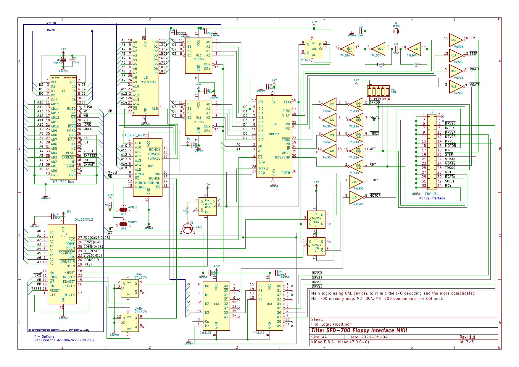
Schematic

Programmable Logic
sfd700.vhd, sfd700_Toplevel.vhd, sfd700_pkg.vhd) are in the CPLD/v1.2/ directory of the Gitea repository. The earlier CUPL files for v1.0/v1.1 remain in the CUPL/ directory for reference.
Automated setup and build (recommended)
macOS / Linux — setup_SFD700.sh
chmod +x setup_SFD700.sh ./setup_SFD700.sh
git, curl/wget and DOSBox (for the CUPL toolchain), and sets up Quartus II 13.0sp1 for the CPLD. On Linux, Quartus is installed natively to ~/altera/13.0sp1 (~1.6 GB); on macOS — where no native Quartus exists — the CPLD toolchain runs from a Docker image (sfd700-quartus:13.0sp1) instead. The MAX7000S device package is fetched automatically.
Windows 10 / 11 — setup_SFD700_windows_native.ps1 (native Git Bash, no WSL). From PowerShell:
Set-ExecutionPolicy -Scope Process -ExecutionPolicy Bypass .\setup_SFD700_windows_native.ps1
bash) and DOSBox, then installs Quartus II 13.0sp1 natively to C:\altera\13.0sp1 together with the MAX7000S package. The build scripts run under Git Bash. To use Docker for the CPLD toolchain instead of native Quartus, set $env:SFD700_CPLD_METHOD = "docker" before running the script.
https://git.eaw.app/eaw/SFD700.git) and an install directory, then offers to build the CUPL/GAL logic (./build_cupl.sh) and the CPLD/VHDL bitstream (./build_cpld.sh). The CUPL build writes SFD700_1.JED and SFD700_2.JED into CUPL/ for a TL866 / XGecu programmer; the CPLD build writes CPLD/v1.2/build/output_files/sfd700.pof for JTAG programming with a USB-Blaster.
GAL (v1.0 / v1.1)
Devices| Device | Package | Macrocells | Registered Outputs | Role |
|---|---|---|---|---|
| GAL26CV12 | 28-pin DIP | 12 | 12 | I/O decoder, FDC control, MZ-700 memory management |
| GAL16V8 | 20-pin DIP | 8 | 8 | ROM address decode, mode select, DRQ multiplexer |
SFD700_GAL1) is the primary logic device. It decodes the Z80 I/O address bus to generate all FDC control signals, manages the bidirectional data bus buffer, tracks MZ-700 memory paging state, and controls the interrupt enable flag.
I/O Address DecodingEight address lines (A0–A7) are combined with the IORQn, RDn, and WRn control inputs to identify each register access. Separate read and write selects are generated for the WD1773 FDC register block so that the bidirectional bus buffer can be switched in the correct direction: IOBUSDIRn goes low (Z80→FDC direction) only on FDC reads, and the FDCn chip select is asserted on both reads and writes. FDC Peripheral Control
Writes to 0xDC, 0xDD, and 0xDE produce single-cycle strobe outputs (DRIVEn, SIDEn, DDENn) that clock the drive selection, head side, and data density latches on the PCB. The FDCRESETn output is tied directly to the Z80 RESET signal so the WD1773 is always reset on system power-up or hardware reset. MZ-700 Memory Management
The MZ-700 uses I/O writes to ports 0xE1–0xE6 to bank its internal DRAM and CGROM in and out of the upper address space. The GAL tracks two independent state bits using its registered outputs, clocked by the decoded port strobes:
- DISROM — set by writes to 0xE3/0xE4, cleared by 0xE1 and by RESET. When set it signals that the host has mapped its DRAM over the card's ROM window.
- INHROM — set by writes to 0xE5, cleared by 0xE6 and by RESET. When set it inhibits the card's ROM entirely, regardless of DISROM state.
The INTEN registered output is clocked by the INTCLK strobe generated from an access to port 0xE7. A write sets the enable (INTEN.D follows !WRn); a read clears it. INTEN is asynchronously reset by the system RESET input. The INTCLK output feeds the clock input of an external flip-flop on the PCB.
| Pin | Signal | Dir | Description |
|---|---|---|---|
| 1 | CLK | In | Registered output clock |
| 2–6, 8–11 | A0–A7 | In | Z80 I/O address bus |
| 11 | IORQn | In | Z80 I/O request (active low) |
| 12 | WRn | In | Z80 write strobe (active low) |
| 13 | RDn | In | Z80 read strobe (active low) |
| 28 | RESET | In | System reset (active high) |
| 15 | DISROMSET | Out | ROM-disable set strobe (active low) |
| 16 | DISROMCLR | Out | ROM-disable clear strobe (active low) |
| 17 | INTCLK | Out | Interrupt enable flip-flop clock |
| 18 | INROMHSET | Out | ROM-inhibit set strobe (active low) |
| 19 | INTEN | Out | Interrupt enable registered output (active low) |
| 20 | IOBUSDIRn | Out | Bus buffer direction — low = Z80→FDC |
| 22 | INHROMCLR | Out | ROM-inhibit clear strobe |
| 23 | SIDEn | Out | Head side select strobe (active low) |
| 24 | FDCRESETn | Out | WD1773 reset (active low, tied to RESET) |
| 25 | DDENn | Out | Double-density enable strobe (active low) |
| 26 | DRIVEn | Out | Drive select strobe (active low) |
| 27 | FDCn | Out | WD1773 chip select (active low) |
SFD700_GAL2) handles the memory-side address decoding: it generates the ROM chip select when the Z80 addresses the firmware window at 0xF000–0xFFFF, and multiplexes address lines onto the ROM to select the correct firmware page and handle the MZ-80A DRQ trick.
ROM Chip SelectMREQn and RDn are combined with the high address lines (A12–A15) to detect accesses to 0xF000–0xFFFF. The ROMCSn output is a registered value so that chip-select glitches caused by address bus settling are suppressed — the select only propagates on the clock edge. ROM Address Multiplexing
Two additional outputs drive ROM address lines beyond A9:
- ROMA15 — driven from the MODESEL1 jumper input, it selects between two firmware images (MZ-700 page and MZ-80A page) stored in the upper and lower halves of the ROM address space.
- ROMA10 — this is the most complex output. On MZ-80A targets (MODESEL1 low) it is multiplexed with the WD1773 DRQ signal: when the ROM is selected and DRQ is asserted, ROMA10 selects one 1 KB mirror of the read routine; when DRQ is not asserted it selects the other mirror containing the wait/retry path. This allows the 2 MHz Z80 to service FDC data transfers via a simple linear jump through ROM rather than a polled software loop it cannot execute fast enough. On MZ-700 targets (MODESEL1 high), ROMA10 is driven directly from DRQ without the address qualification.
SFD700_2.PLD.MZ700— simplified ROMA10 logic: output follows DRQ directly.SFD700_2.PLD.MZ80A— full multiplexed ROMA10 with address qualification and commented-out output-enable controls used during development.
| Pin | Signal | Dir | Description |
|---|---|---|---|
| 1 | CLK | In | Registered output clock |
| 2–7 | A10–A15 | In | Z80 high address bus |
| 8 | MREQn | In | Z80 memory request (active low) |
| 9 | RDn | In | Z80 read strobe (active low) |
| 12 | MODESEL0 | In | Mode jumper bit 0 |
| 13 | MODESEL1 | In | Mode jumper bit 1 — selects ROM page / DRQ logic |
| 14 | ROMINH | In | ROM inhibit state from GAL1 |
| 15 | ROMDIS | In | ROM disable state from GAL1 |
| 16 | DRQ | In | WD1773 data request |
| 17 | ROMA15 | Out | ROM address bit 15 (firmware page select) |
| 18 | ROMA10 | Out | ROM address bit 10 (DRQ multiplexer on MZ-80A) |
| 19 | ROMCSn | Out | ROM chip select (active low, registered) |
CUPL/ directory can be used directly without recompilation.
To recompile from source, use the batch scripts included in the CUPL/ directory:
# Compile GAL1 (GAL26CV12) — run inside CUPL directory cupl -j -f -a g26cv12 SFD700_1 # Compile GAL2 (GAL16V8) cupl -j -f -a g16v8 SFD700_2
-j flag produces JEDEC output (.JED), -f produces the fuse plot (.DOC), and -a <device> specifies the target device. Compiled outputs are written to the same directory:
SFD700_1.JED— JEDEC fuse file for GAL1, ready for programming.SFD700_2.JED— JEDEC fuse file for GAL2, ready for programming.SFD700_1.DOC/SFD700_2.DOC— human-readable fuse plots and chip diagrams for verification.SFD700_1.ABS/SFD700_2.ABS— binary intermediate files used by some programmer utilities.
The GAL16V8 is supported natively by virtually all modern device programmers. Using a TL-866 II+ or similar with the open-source
minipro utility:
minipro -p GAL16V8 -w SFD700_2.JED
SFD700_G.JED) is also provided in the CUPL/ directory for direct use. Verify after programming with:
minipro -p GAL16V8 -v SFD700_2.JED
The GAL26CV12 is a 28-pin PLCC/DIP device that is not listed in the standard TL-866 II+ device database. Programming requires a PLCC-28 to DIP-28 adapter and a custom device entry in the Minipro
infoic.xml database — a pre-configured infoic.xml is included in the CUPL/ directory. With the adapter fitted and the custom database in place:
minipro -p GAL26CV12 -w SFD700_1.JED
.JED file directly — all compliant GAL programmers accept the JEDEC 3C format that CUPL produces.
Both GAL devices retain their programmed configuration in EEPROM and are ready immediately at power-on with no load delay. They can be erased and reprogrammed in-circuit if JTAG test points are provided, or removed from their sockets for bench programming.
CPLD
Device| Resource | Used | Available | Utilisation |
|---|---|---|---|
| Macrocells | 72 | 128 | 56% |
| Registers | 37 | 128 | 29% |
| I/O pins | 65 | 68 | 96% |
| Product terms | 179 | — | — |
| Global clocks | 2 | 2 | 100% |
CLK_16M (the primary clock) and Z80_RESETn (synchronous reset), minimising clock and reset skew across the device.
Clock GenerationThe on-board 16 MHz crystal oscillator drives the
CLK_16M global clock input. A single registered toggle macrocell divides this by two to produce CLK_FDC, the 8 MHz clock fed directly to the WD1773 FDC chip-clock input.
I/O Address DecoderPurely combinatorial logic decodes Z80 I/O cycles (IORQn asserted with RDn or WRn) across three address blocks: the WD1773 FDC registers at 0xD8–0xDB, the FDC control registers at 0xDC–0xDF, and the paging and mode registers at 0x60–0x63. On MZ-700 and MZ-1500 targets (MODE 1 and 4) the decoder also captures writes to I/O ports 0xE0–0xE6 to track the host memory management state. The maximum fan-out node in the design originates from the address decode tree and drives 67 macrocell inputs. Memory Address Decoder
Decodes Z80 memory cycles (MREQn with RDn or WRn) to generate active-low chip-select outputs for the on-board Flash ROM (
ROM_CSn) and static RAM (RAM_CSn). Two independent 7-bit page registers — EXXX_PAGE (loaded via 0x60) and FXXX_PAGE (loaded via 0x61) — are driven onto address bits ROM_A10 and RAM_A10, bank-switching 4 KB windows within up to 512 KB of addressable storage.
Drive and Motor ControlA write to I/O port 0xDC loads an 8-bit registered value that drives the four active-low drive-select outputs (DRVSAn–DRVSDn) and the motor-enable line (MOTOR). Bits [2:0] encode the selected drive (values 4–7 select drives A–D; 0 deselects all); bit 7 controls the spindle motor. Head-side selection (0xDD) and double-density mode (0xDE) are managed by separate single-bit registers. Data Bus Inversion and Multiplexing
The WD1773 requires bitwise-inverted data. The CPLD connects to a dedicated 8-bit inverted data bus (
ID[7:0]) and handles the polarity inversion transparently in both read and write directions. On a Z80 read of an FDC register the inverted bus is re-inverted onto the Z80 data bus; on a write to an FDC register the Z80 data bus is inverted onto ID[7:0]. When a page register is read back by the host, the CPLD drives the stored page value directly onto the Z80 data bus instead.
On MZ-80A and MZ-1200 targets (MODE 0) the WD1773 DRQ signal is multiplexed onto Flash ROM address bit A10 (ROM_A10). Each 1 KB segment of the boot ROM contains a mirrored copy of the read routine; the DRQ state selects the correct copy directly, bypassing the software polling loop that the 2 MHz Z80 cannot execute fast enough to service the FDC data rate reliably.
Interrupt ControlThe WD1773 INTRQ output is gated by a single registered enable bit. A write to I/O port 0xDF enables routing of INTRQ to the Z80 INT line; a read from 0xDF clears the enable. A secondary output, Z80_EXWAITn, is available to insert external wait states during FDC register access if required by host timing. MZ-700 / MZ-1500 Memory Management
The MZ-700 and MZ-1500 use I/O writes to 0xE0–0xE6 to bank their internal DRAM and ROM in and out of the upper address space. The CPLD monitors these writes and maintains a two-bit state register: writing 0xE5 sets the inhibit state, suppressing
ROM_CSn and RAM_CSn regardless of page register contents; writing 0xE3, 0xE4, or 0xE6 clears the inhibit and re-enables the expansion card windows.
Mode RegisterThree mode jumper inputs (MODE[2:0]) are sampled and latched into a registered value on the rising edge of Z80_RESETn. Reading I/O port 0x63 returns this value, allowing boot firmware to auto-detect the host machine without DIP switches or manual configuration.
| Signal | Pin | Direction | Description |
|---|---|---|---|
| CLK_16M | 83 | In | 16 MHz crystal oscillator — global clock |
| CLK_FDC | 81 | Out | 8 MHz clock to WD1773 |
| CLK_BUS0 | 2 | In | Host Z80 bus clock |
| Z80_RESETn | — | In | Active-low reset — global resource, latches MODE |
| A[15:0] | 4–25 | In | Z80 address bus |
| D[7:0] | 27–35 | Bidir | Z80 data bus |
| ID[7:0] | 64–74 | Bidir | Inverted data bus (WD1773 side) |
| M1n | 36 | In | Z80 M1 machine-cycle indicator |
| RDn | 37 | In | Z80 read strobe |
| WRn | 39 | In | Z80 write strobe |
| IORQn | 40 | In | Z80 I/O request |
| MREQn | 41 | In | Z80 memory request |
| Z80_INT | 44 | Out | Interrupt output to Z80 (gated INTRQ) |
| Z80_EXWAITn | 45 | Out | External wait request to Z80 |
| FDCn | 63 | Out | WD1773 chip select (active low) |
| INTRQ | 61 | In | WD1773 interrupt request |
| DRQ | 60 | In | WD1773 data request |
| DDENn | 58 | Out | Double-density enable to WD1773 (active low) |
| SIDE1 | 57 | Out | Head side select |
| MOTOR | 56 | Out | Spindle motor enable |
| DRVSAn | 55 | Out | Drive A select (active low) |
| DRVSBn | 54 | Out | Drive B select (active low) |
| DRVSCn | 52 | Out | Drive C select (active low) |
| DRVSDn | 51 | Out | Drive D select (active low) |
| ROM_CSn | 77 | Out | Flash ROM chip select (active low) |
| RAM_CSn | 76 | Out | Static RAM chip select (active low) |
| ROM_A10 | 80 | Out | ROM page address bit / DRQ mux (MZ-80A MODE) |
| RAM_A10 | 79 | Out | RAM page address bit |
| MODE[2:0] | 49,48,50 | In | Host machine mode jumpers |
git clone https://git.eaw.app/eaw/SFD700 cd SFD700/CPLD/v1.2/build
quartus_map --read_settings_files=on sfd700 # Analysis & Synthesis quartus_fit --read_settings_files=on sfd700 # Fitter (Place & Route) quartus_asm --read_settings_files=on sfd700 # Assembler — generates sfd700.pof quartus_sta sfd700 # Timing analysis (optional)
CPLD/v1.2/build/sfd700.qpf in the Quartus II GUI and use Processing → Start Compilation. On a successful build the output programming file is written to:
CPLD/v1.2/build/output_files/sfd700.pof
EPM7128SLC84-15 (MAX7000S family) in the Quartus project settings.
quartus_pgm -c "USB-Blaster" -m JTAG \ -o "p;CPLD/v1.2/build/output_files/sfd700.pof"
- Open Tools → Programmer.
- Click Hardware Setup and select USB-Blaster.
- Click Add File and select
output_files/sfd700.pof. - Tick Program/Configure and optionally Verify.
- Click Start. Programming completes in a few seconds.
I/O Register Map
| Port | R/W | Description |
|---|---|---|
| 0xD8–0xDB | R/W | WD1773 FDC registers (Status, Command, Track, Sector, Data). |
| 0xDC | W | Drive & motor: bits [2:0] select drive (4=A, 5=B, 6=C, 7=D, 0=none); bit [7] controls motor. |
| 0xDD | W | Head side: D0=0 → side 1, D0=1 → side 0. |
| 0xDE | W | Data rate: D0=0 → double density, D0=1 → single density. |
| 0xDF | W/R | Interrupt: write → enable WD1773 INT to host; read → disable WD1773 INT. |
| 0x60 | R/W | EXXX page register: D7 selects storage (0=Flash ROM, 1=RAM); bits [6:0] select a 4 KB page mapped into E300:EFFF. |
| 0x61 | R/W | FXXX page register: D7 selects storage (0=Flash ROM, 1=RAM); bits [6:0] select a 4 KB page mapped into F000:FFFF. |
| 0x63 | R | Mode register: reads back the MODE jumper value (0–6). |
| 0xE1 | W | MZ-700/MZ-1500 only: disable onboard ROM (host maps DRAM to D000:FFFF). |
| 0xE3, 0xE4 | W | MZ-700/MZ-1500 only: re-enable onboard ROM. |
| 0xE5 | W | MZ-700/MZ-1500 only: inhibit all onboard ROM/RAM access. |
| 0xE6 | W | MZ-700/MZ-1500 only: clear ROM inhibit, re-enable onboard ROM/RAM. |
Memory Map
| Window | Address Range | Page Register | Notes |
|---|---|---|---|
| EXXX | E300:EFFF | 0x60 | E000:E2FF is reserved for MZ-700/MZ-1500 memory-mapped I/O, so only 3.75 KB of the 4 KB page is usable by firmware (RFS). |
| FXXX | F000:FFFF | 0x61 | Full 4 KB window. Default page 0 holds the MZ-80A AFI ROM; default page 1 holds the MZ-700 AFI ROM. |
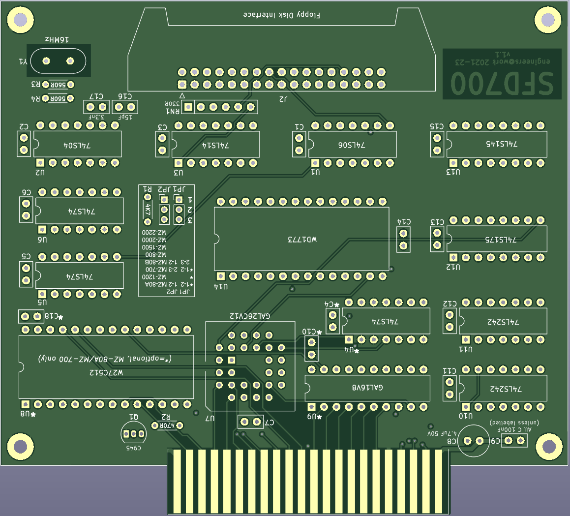
PCB
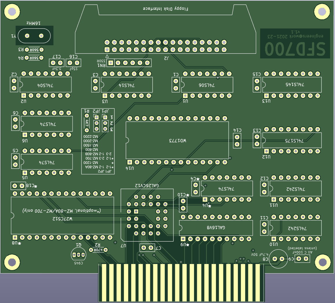
v1.1 PCB
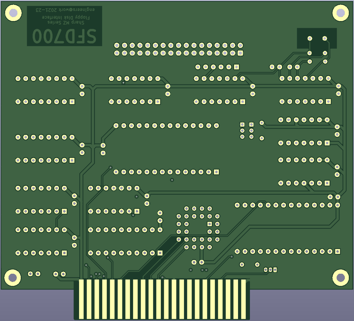
The PCB is more complex than the SFD-800 as it requires a CPLD, ROM/RAM storage and additional support circuitry (earlier v1.0/v1.1 revisions used two GAL devices instead of the CPLD).

v1.2 PCB

Manuals
| Manual | Description |
|---|---|
| User Manual | Board overview, MODE jumper setup, drive installation, ROM Filing System usage, and troubleshooting |
| Technical Guide | Hardware architecture, CPLD design, I/O register map, memory map, and build/programming procedures |
| Developer’s Guide | Full VHDL source code walkthrough with VHDL explained for non-VHDL programmers, process-by-process analysis, and CPLD modification guide |
Documentation
The above link downloads the original K&P SFD-800 User Manual which is relevant to this design. It is in German so for non German speakers, the best way to translate is to use your smart phone, load the Google translate app, set to realtime camera translate and set the language as German-><your language>.
Files
Please see Gitea for all project files.
The v1.2 PCB Gerbers are available in the releases/ directory of the Gitea repository. Six spare v1.2 boards are available — contact via the website if interested, postage cost only.
Credits
The SFD-700 mkII is a new design inspired by the original concept. The PCB layout, schematic and programmable logic (CUPL for v1.0/v1.1; VHDL for v1.2) were written from scratch. It is not a direct replica — the host-mode logic, ROM/RAM paging and MZ-80A DRQ-to-address-line adaptation are original additions not present in the K&P product.
Licenses
The Gnu Public License v3
The source files are distributed in the hope that it will be useful, but WITHOUT ANY WARRANTY; without even the implied warranty of MERCHANTABILITY or FITNESS FOR A PARTICULAR PURPOSE. See the GNU General Public License for more details.
You should have received a copy of the GNU General Public License along with this program. If not, see http://www.gnu.org/licenses/.