 tranZPUter SW-700
Foreword
The project aims to provide the same functionality to the Sharp MZ-700 as is now provided on the Sharp MZ-80A.
The Sharp MZ-700 is a more compact design which required a new solution for upgrading it's CPU and Video. It wasnt possible, without hardware hacks, to upgrade the existing video and with limited internal space presented more of a challenge. I eventually settled on a combined board where the tranZPUter SW and Video Module designs were used but with less components and a co-existence of the new enhanced video with the original. This solution allows the machine to run as original or with selectable enhanced features as required. It is a more wholesome solution with many possibilites beyond enhancing the MZ-700, for example it would be quite easy to run Linux on this machine, either via the on-board K64F processor using the host as a terminal and/or reprogramming of the CPLD/FPGA to instantiate a soft-cpu and creating a development station for any conceivable processor, so would be of great use to students studying microprocessors and FPGA's.
The design is still being developed and these pages will be updated as new information becomes available. The reader is encouraged to read the seperate sections on the tranZPUter, tranZPUter SW and Video Module to gain an understanding of the tranZPUter SW-700 evolution.
Everything will be written in C/C++ (FLW - Famous Last Words - I had to write the interrupt service routines in ARM Thumb assembler for the original tranZPUter SW as the K64F wasnt quite powerful enough using compiled C).
Overview
The upgrade also extends the Z80 hardware capabilities by providing additional RAM to allow for a 64K version of CP/M v2.2 (and upto 512K CP/M v3 when I get around to porting it) and to increase the speed of the processor whilst maintaining the original speed when accessing the Sharp MZ-700 motherboard peripherals.
This design is a work in progress, albeit now mature and stable, it is working in tandem with the tranZPUter, tranZPUter SW and Video Module projects. As updates to the aforementioned projects are made or viz-a-viz, they are back ported to this design. The C/C++ control software written for the tranZPUter SW is common and also intended to work on the tranZPUter under the ZPU.
tranZPUter SW-700
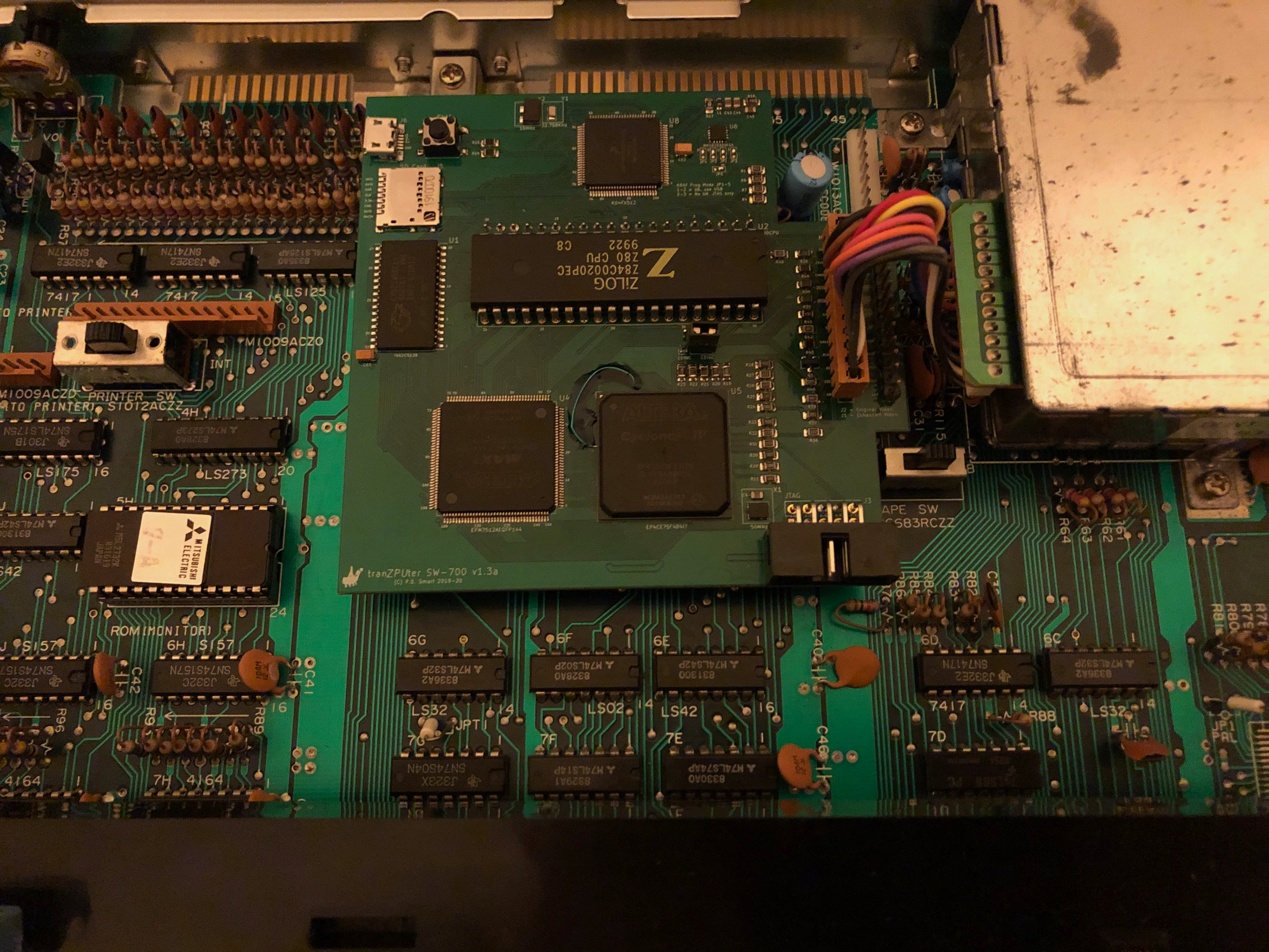
The tranZPUter SW-700 follows on from the tranZPUter / tranZPUter SW designs and in addition adding the Video Module functionality to upgrade the host video. It also upgrades the underlying Z80 hardware enabling higher performance and increased memory. It embeds a Freescale K64F ARM Cortex-M4 in place of the ZPU Evo as the tranZPUter SW-700 is more a software solution to the requirement rather than the ZPU Evo which is based on VHDL on an FPGA. The project adds the suffix SW-700 for SoftWare for the MZ-700 to distinguish the designs.
The design of the tranZPUter SW-700 upgrades the Z80 hardware and can clock the processor, detached from the Sharp MZ-700 motherboard, at much higher clock rates, reliably tested and verified at 24MHz by overclocking a Z84C0020 20MHz CPU. Higher CPU performance will be a benefit to programs such as CP/M or databases such as DBase II.
To provide different CPU's you have the choice of taking existing ARM based software CPU emulations, for example those used in the PiCoPro and adapting them to use the CPU signals on the MZ-700 bus via this designs interface or hardware based 'soft' processors instantiated on the FPGA. The program memory could be either: the MZ-700 motherboard 64K; the tranZPUter 512K; the faster K64F 256K memory; FPGA BRAM or any combination. There is no real need to use the MZ-700 memory when using a soft/'soft' CPU except for perhaps cache purposes. The benefits of using a soft/'soft' CPU with local K64F/FPGA RAM is better performance and access to alternative software.
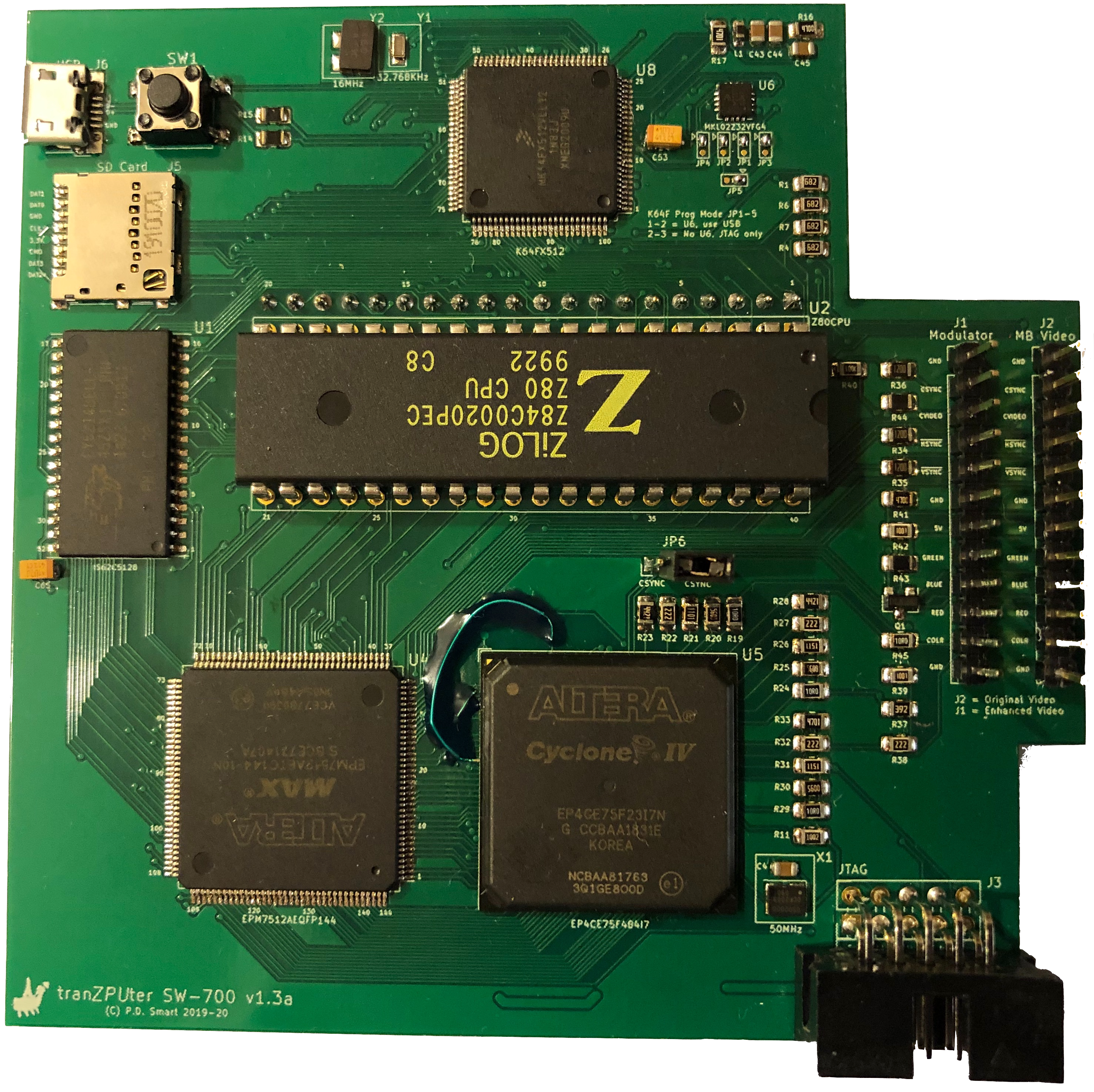
In the gallery are pictures of the current design, files have been uploaded onto github and are relatively stable, WIP files wont be uploaded as they are in constant flux.
Hardware
Bus mastering is used to take control of the Z80 bus and to transfer data between main memory and an SD Card or between the I/O processor and the Video display buffer for presentation of menu's. It is also used where a soft processor completely idle's the hard Z80 and acts as the main computer CPU. ie. using a soft CPU emulator, it can process applications in local memory and slow down to access I/O and the Video buffer (if running with original video, the enhanced video runs at full speed) on the host machine as needed presenting a completely different computing experience. Imagine, a 6809 or a 68000 based Sharp MZ-700!
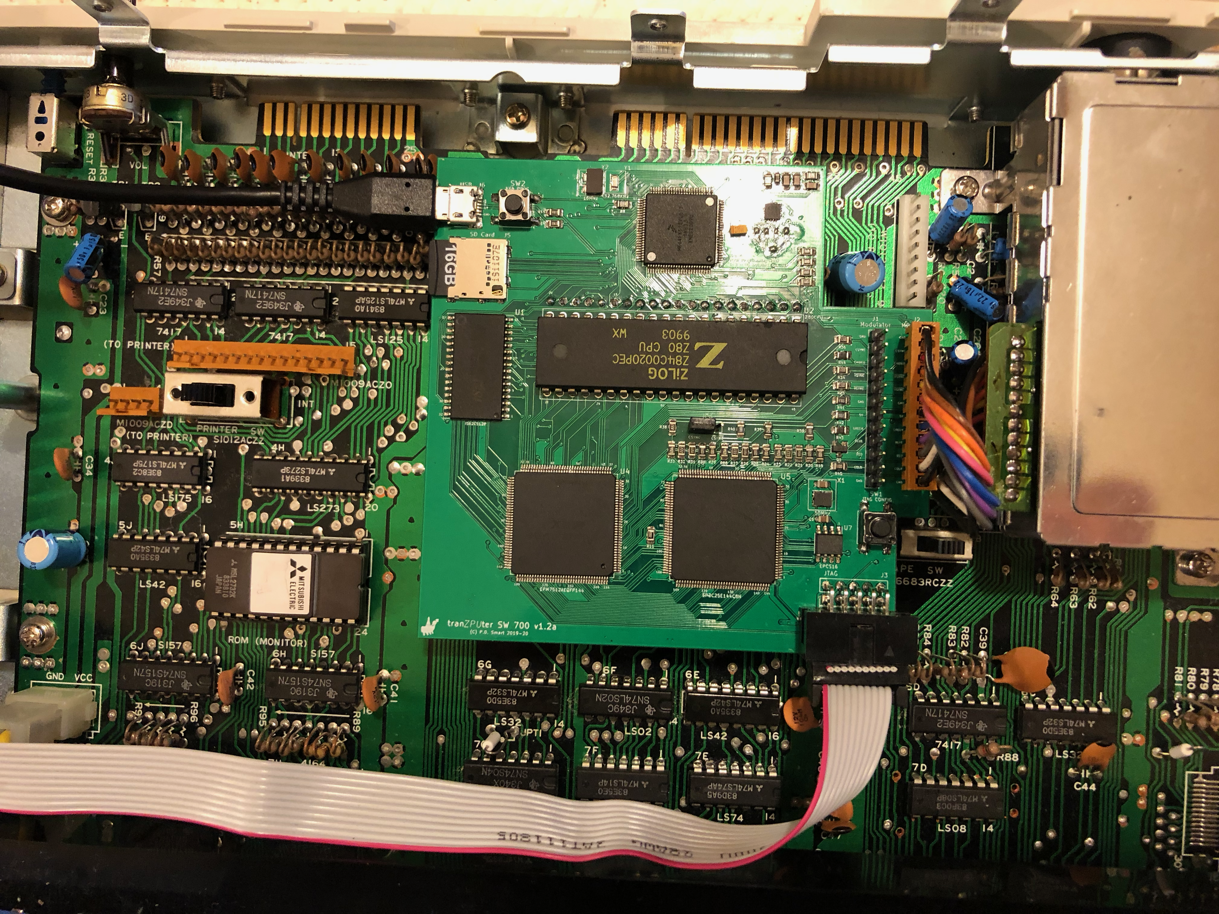
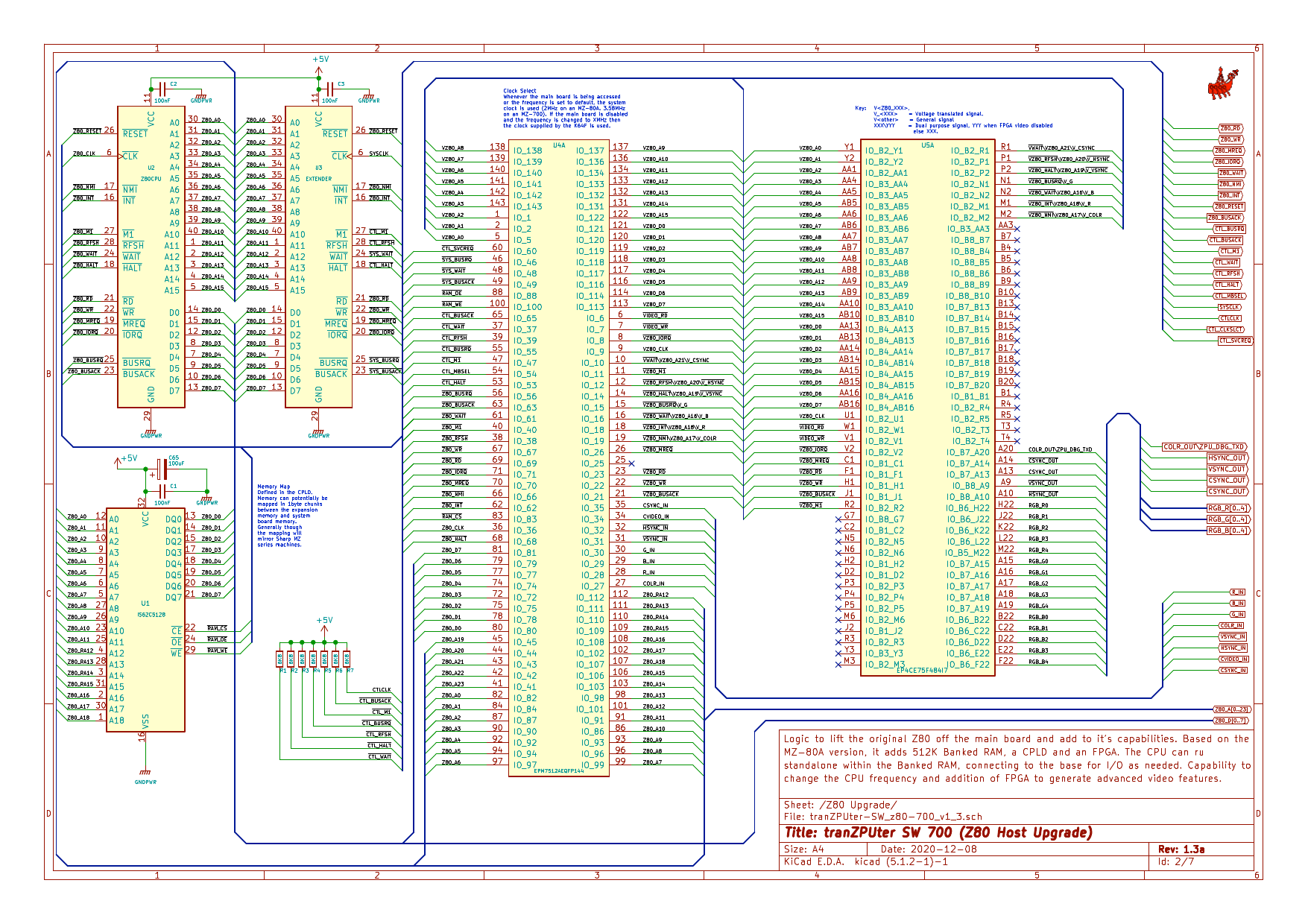
The design centres around lifting the original Z80 onto a daughter card and rerouting several of its signals such that they can be controlled as needed. It also takes video output from the mainboard and routes it internally to the FPGA based video module, where original or enhanced video can be selected before it is rerouted to the modulator via a new connector.
Design versions v1.0 and v1.1 were internal designs and wont appear in the repository. v1.2 was the first design which went on to be assembled and tested on the MZ-700. This design was used to further the software and FPGA development and verify stability and reliability. v1.3 is now the mainstream design, based on a more powerful FPGA, a Cyclone IV 75K (or a Cyclone IV 115K - build time selectable) which allows for higher resolution graphics and the ability to utilise alternate 'soft' hardware based processors, specifically the Z80 clone, T80 and the ZPU Evolution.
v1.2 and v1.3, with fundamental differences in logic and software, maintain their own branches in git. Both are proven designs, with v1.2 being cheaper to produce.
v1.2 Schematics
Version 1.2 is the first official release of the tranZPUter SW-700 design. It is based around the Sharp MZ-80A tranZPUter SW v2.2 and the Video Module v2.0 with optimisations to fit the Sharp MZ-700 platform.
v1.2 Z80 Upgrade Schematic
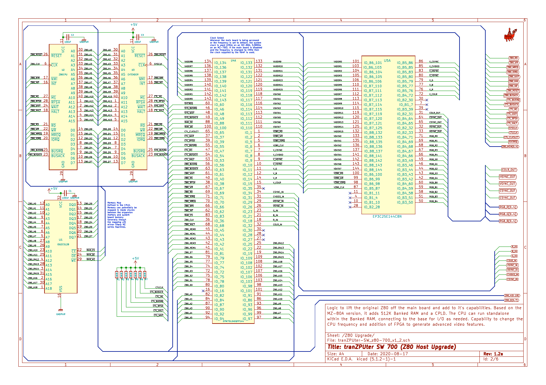
The above schematic has been designed such that the board can be installed into an MZ-700 and the CPLD will be configured such that the machine is original, ie. no additional features enabled on power up. A write by the Z80 to the CPLD I/O registers can enable features as required. This fulfills the requirement of keeping the machine original to maintain maximum compatibility with software.
v1.2 The K64 I/O Processor
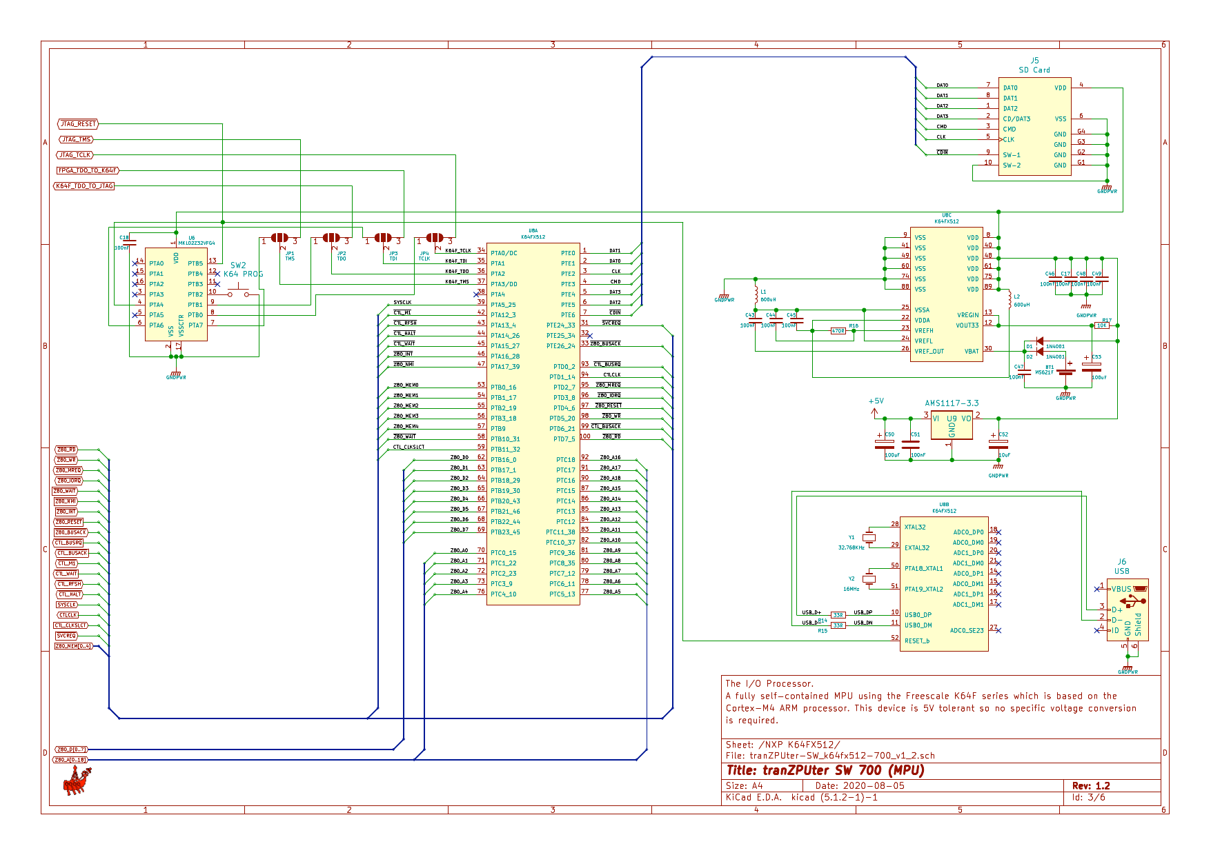
In order to provide embedded debugging, development and learning tools, enhanced features such as an SD card, soft-processors and offloaded co-processor services, an Freescale K64F ARM Cortex-M4 CPU is added into the design. This processor has all the necessary hardware connectivity with the CPLD/Z80 giving it the ability to read or control any aspect of the tranZPUter SW-700 board or the MZ-700 mainboard. Under default conditions the K64F interacts with the Z80 to load the TZFS enhanced monitor, provide an SD drive and aid in providing the alternate MZ series emulations such as the MZ-80A.
As the K64F utilises zOS as it's embedded OS, a USB connection can be made to the MZ-700 and a user can interact with an embedded session to change CPU frequency, edit/dump memory, change registers etc. This feature is ideal for learning how a computer works or for debugging Z80/ARM code.
An optional feature is the installation and use of the PJRC bootstrap MCU which allows updating the K64F firmware via a USB cable. Without this MCU, the JTAG interface has to be used along with a compatible Open SDA interface such as the one provided on the Freescale FRDM-K64F development board to update the K64F firmware. To allow for this optional device there are a set of 5 solder jumpers, connecting pads 1-2 on JP1-5 allows programming and use of the PJRC MCU, connecting pads 2-3 on JP1-4, pins 1-2 on JP5 enables programming via the JTAG interface using the SWD protocol.
To power the K64F a seperate 3.3V regulator is used. It was intentionally chosen to use a seperate LDO to power the K64F rather than combining with the CPLD/FPGA requirements and use a larger LDO.
NB. A zOS application is being developed to flash new firmware into the K64F via the zOS console from the SD card and will remove the need to use the PJRC or JTAG tools. This tool should be available in zOS v1.2.
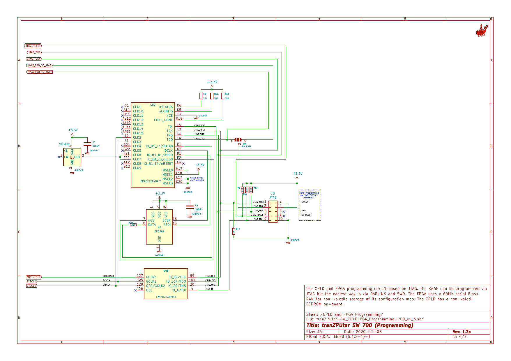
v1.2 JTAG Programming and Oscillator
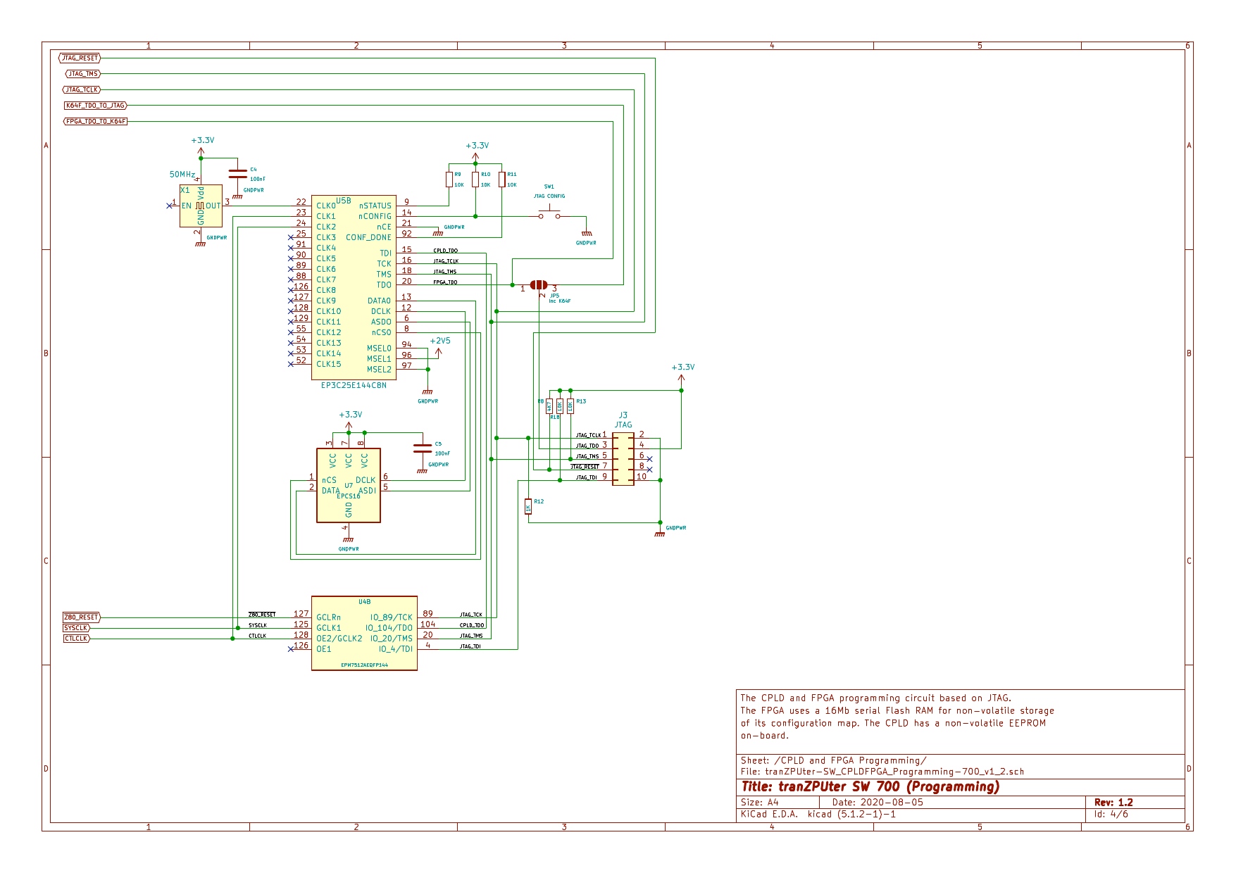
This design uses a CPLD and an FPGA both of which require programming via a JTAG interface. Using Altera best-practice the JTAG interface is wired to the highest voltage device first (CPLD) and daisy chained to the lower voltage FPGA. The recommended pull-up/down resistors are as per Altera specifications.
The FPGA requires a bit stream to configure its internal logic matrix, which in turn provides the desired hardware functionality. This can be done real-time via a JTAG interface but doesnt solve the issue on power up. This is the reason for the 16Mbit EPCS16 which is connected to the Cyclone III FPGA bootstrap pins. The EPCS16 is programmed via the Cyclone III using an Altera provided IP (Intellectual Property) which converts JTAG programming into EPCS16 programming. Once programmed and upon power up or pressing of the CONFIG switch, the EPCS16 contents are read into the FPGA and configures its logic matrix.
As the FPGA has 4 onboard PLL devices, the main crystal is fed into the Cyclone III FPGA and this acts as the timebase for all internal synchronous signals and video mode clocks. The frequencies used by the Z80, ie. the mainboard frequency SYSCLK and the K64 generated alternate frequency CTLCLK are also fed into the Cyclone III to enable synchronisation.
v1.2 Power Supply
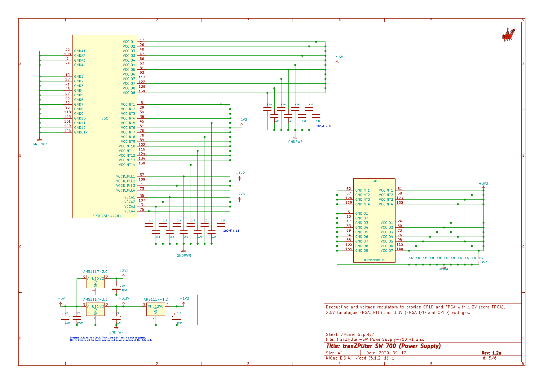
Using more advanced technology requires voltages different to the original 5V standard. The CPLD requires 3.3V to function and the FPGA requires 1.2V for internal operations, 2.5V for analogue and PLL devices and a selectable I/O voltage, which in this design is 3.3V as it interfaces with the CPLD.
In order to generate these voltages, 3 LDO devices are used, each specified to 1A per rail. Using Altera tools the maximum power requirement for the CPLD/FPGA will be met by these LDO devices and by the original Sharp MZ-700 PSU.
Additionally, using CPLD/FPGA devices requires significant decoupling and Altera provide a dynamic spreadsheet to work out the number and value required. This is reflected in the schematic above.
v1.2 Video Interface
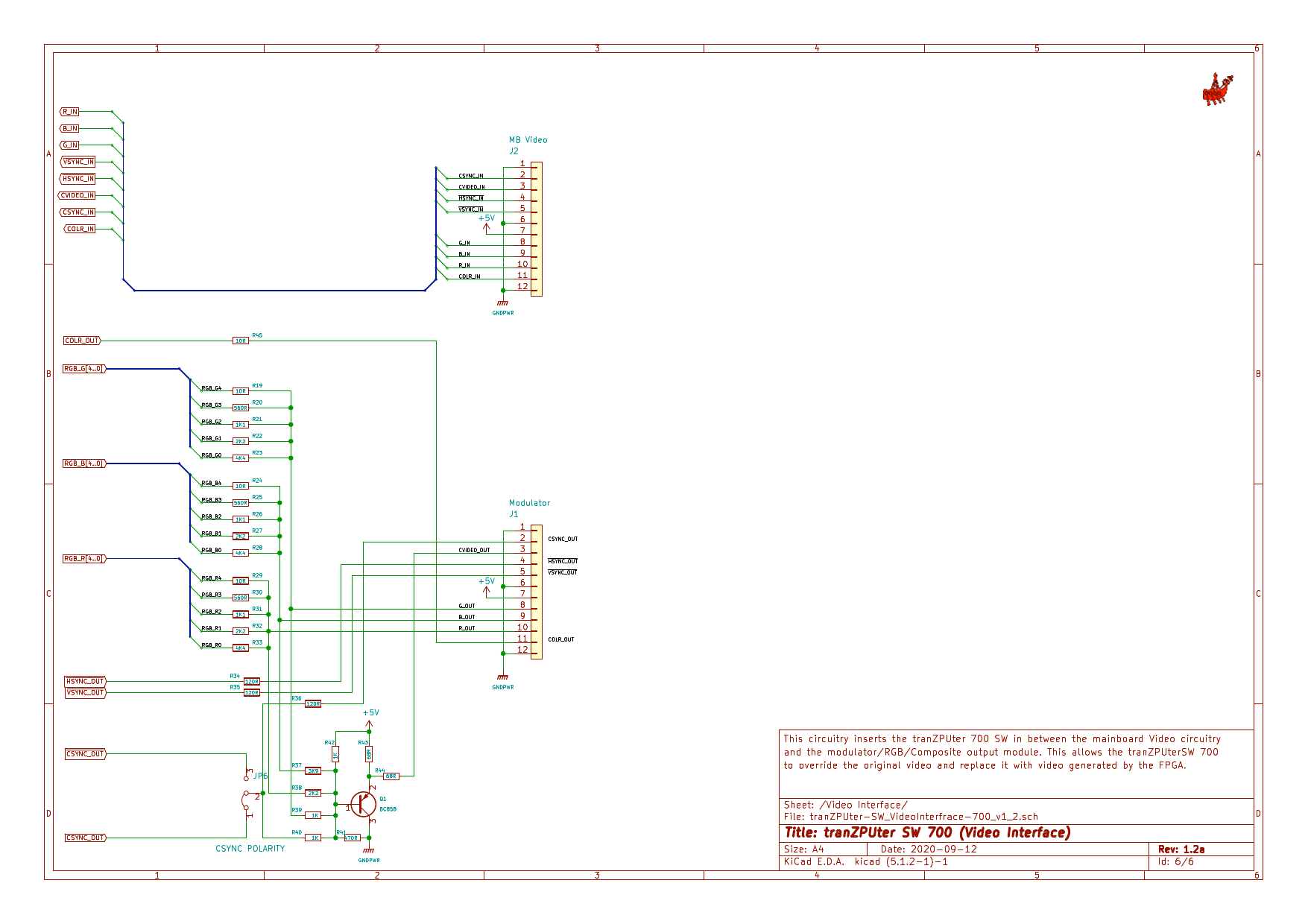
Provision of enhanced video in this design differs from the method used in the Video Module v2.0. It was not possible to uplift existing IC's from the mainboard as most are soldered in place and internal space for expansion is also a big issue. Alternative methods were considered, eventually deciding on a mechanism which not only provided enhanced video from the FPGA but also allowed the original video to remain, switching between the two by software as needed.
Using this mechanism, the video signals are uplifted from the mainboard modulator connector, routed into the FPGA via the CPLD (CPLD is 5V tolerant) and the FPGA either switches the original video to the output or generates it's own video. The CPLD takes care of enabling the mainboard such that when the enhanced FPGA video is being used, the signals to the original video hardware are blocked via the bus tri-state mechanism.
On the Video Module v2.0, 4 bits (3:0) per colour are output to give greater colour depth than the original MZ-700 hardware, which can be either driven directly from video ram attribute bits or via a colour palette lookup table. As this design now has to maintain compatibility with the original modulator a 5th bit per colour has been added so that digital RGB monitors and the circuitry for composite/TV inside the modulator are driven by a voltage > 2V for logical 1 as opposed to the analogue RGB requirements of 0 - 0.75Vp-p. When driving a digital RGB monitor or driving the composite/TV output of the MZ-700 the 5th bit will be activated along with all the other bits therefore ensuring > 2.0V for a digital 1. When driving an analogue RGB monitor the 5th bit cannot be activated as it will over saturate the inputs, BUT if the bit is set to hi-Z or 0 levels then the 5th bit can be used to create a further 16 sets of shades per colour, ie. R[3:0] + 0, G[3:0] + 0, B[3:0] + 0 or R[3:0] + hi-Z, G[3:0] + hi-Z, B[3:0] + hi-Z. This works when the 5th bit is set to 0 as it will act as a current sink for the other 4 bits, dropping the voltage seen by the monitor when the 10R resistor is seen in-circuit. This provides 32 unique voltage levels per colour. When the 5th bit is set to hi-Z (high impedance) there is negligible change in the voltage output from bits 3:0.
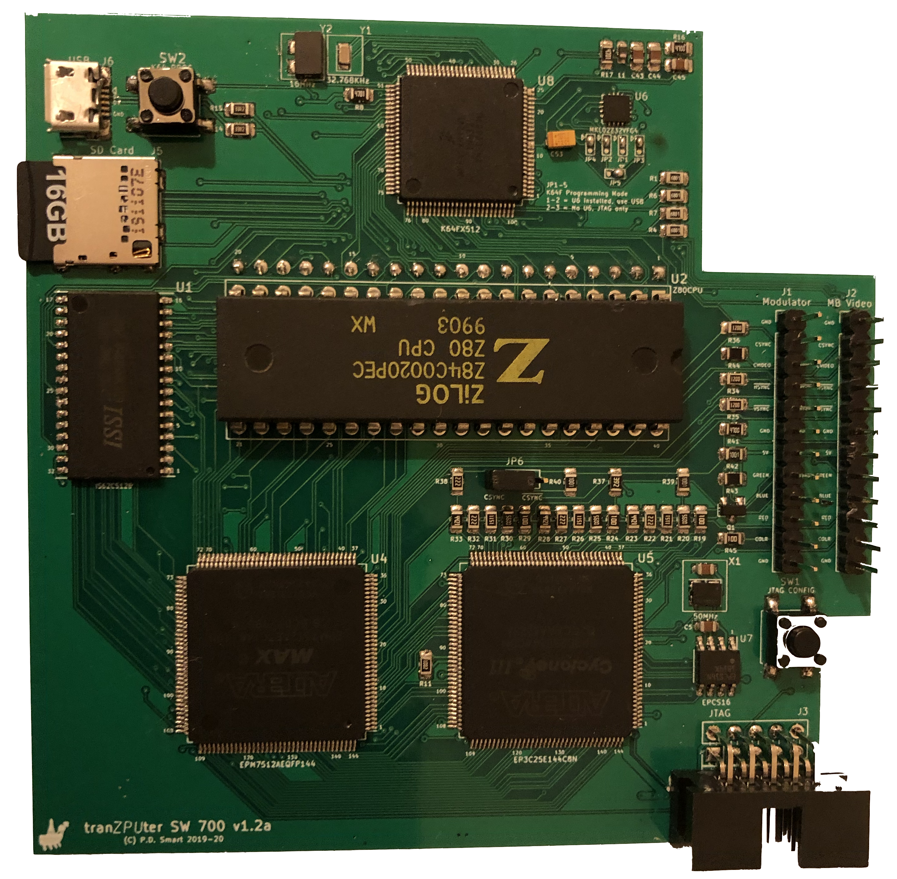
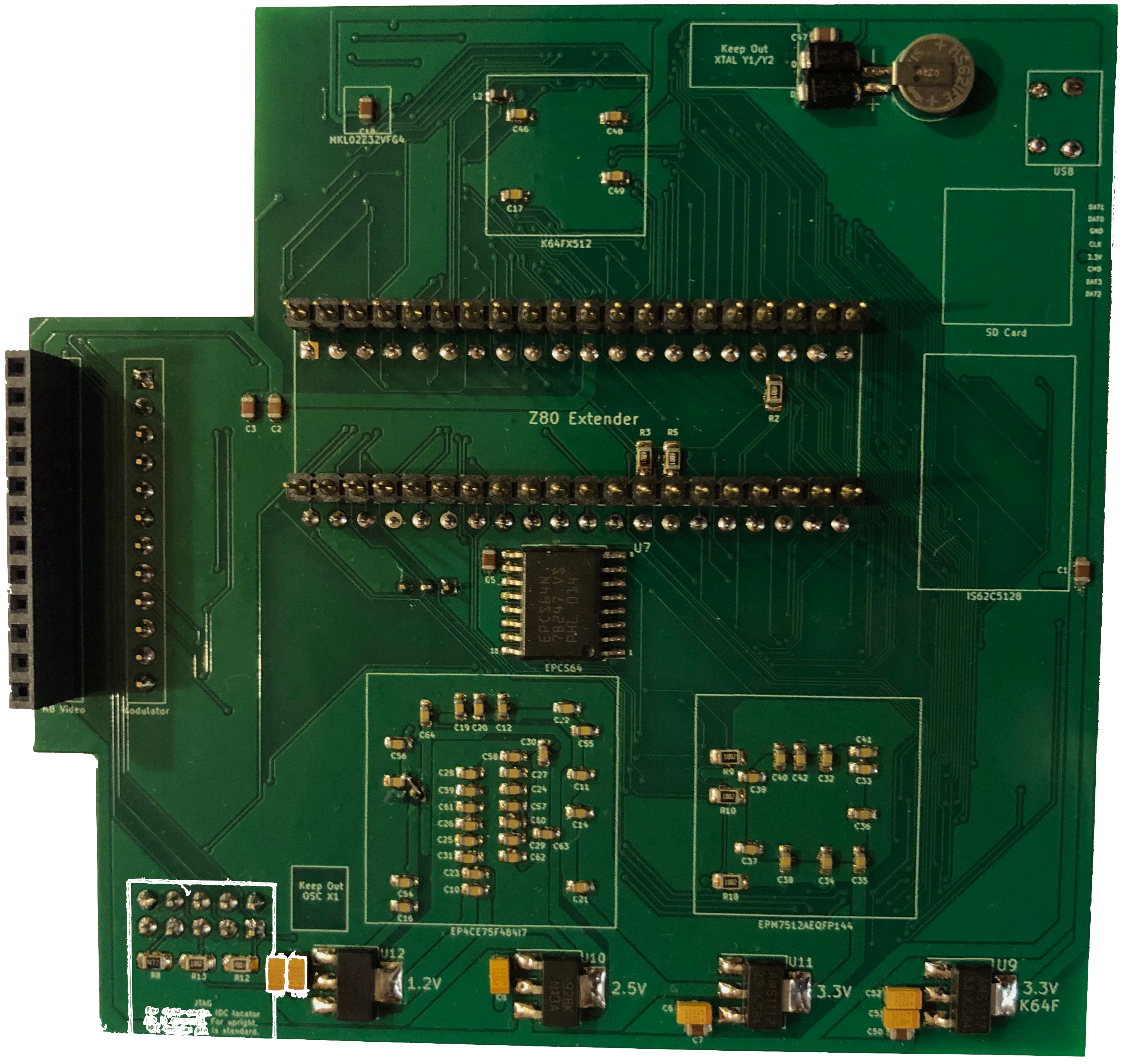
v1.2 PCB
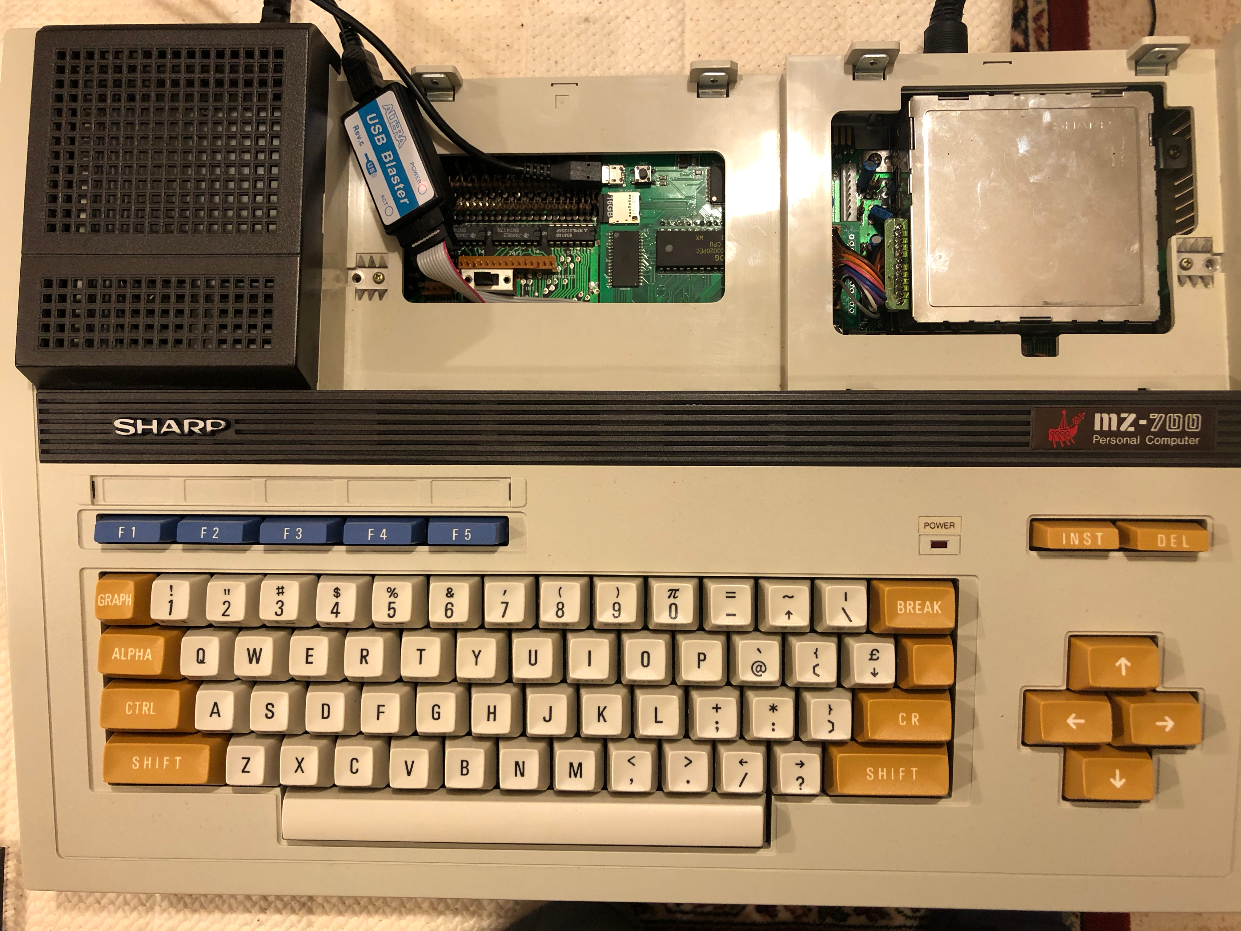
The PCB requirements to fit inside the MZ-700 had to be accurate, in terms of the locations it could be sited to not affect mainboard components, casing obstacles, heat generation etc. Also the board has to fit into the Z80 socket yet at the same time connect to the modulator connector, both would provide the anchor points to keep the board electrically connected and mechanically stable.
This design now uses 3 high density TQFP packages therefore adding more complexities, ie. routing. Space has to be available for all the lands given they are output in a 0.5mm pitch over a large area along with power distribution and decoupling. The board is intentionally kept to 2 layer to gain the best production cost, typically US$60 including stencils for 10 boards, multi-layer would more than double the cost and only gain marginal size reductions.
The board below is a fully assembled and tested PCB for the Sharp MZ-700 along with images showing it installed in the physical machine.
v1.3 Schematics
Version 1.3 takes the working design of v1.2 and changes the FPGA to a more advanced component, the Cyclone IV EP4CE75, a 75K Logic Element device with over 340KB Block RAM. A build time option can use the Cyclone IV EP4CE115, a 115K Logic Element device with over 480K Block RAM. These devices allows for more advanced graphics, higher resolution and more simultaneous colours. It also allows for the creation of ‘soft’ HDL based CPU’s and is a stepping stone to the next iteration of the original ZPU based tranZPUter which will be based entirely on FPGA’s (ie. no Z80, just a Z80 extender socket with the Z80 instantiated as a soft-cpu in the FPGA).
v1.3 Z80 Upgrade Schematic
v1.3 The K64 I/O Processor
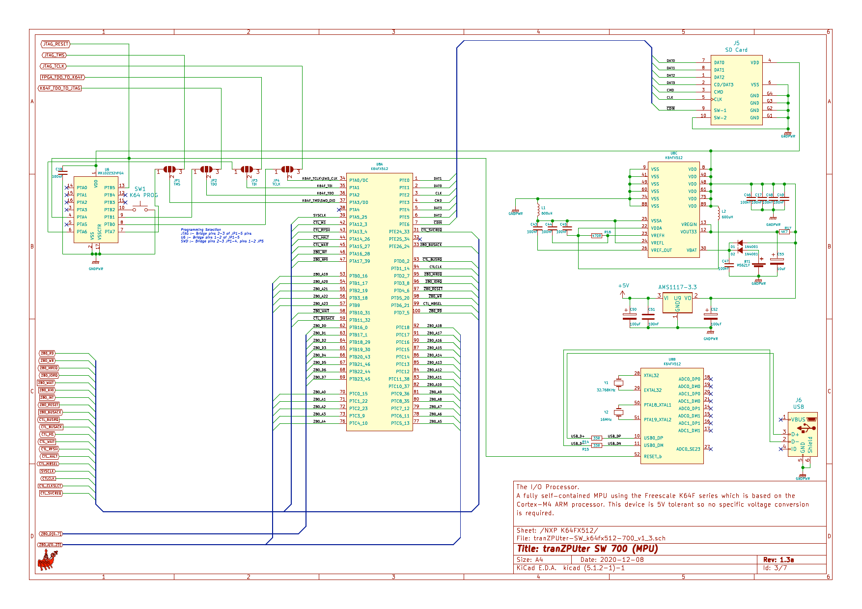
The K64F schematic remains the same as v1.2 with the exception of reworking of the interconnects, removing some which no longer serve a useful function and adding to allow full 24bit direct addressing of memory and FPGA resources.
v1.3 JTAG Programming and Oscillator
Version 1.3 sees the FPGA change and as a consequence, the clock is assigned to different clock inputs. In addition, as the device is larger, it requires a larger boot device in the form of the EPCS64, a 64mbit serial flash ram. As the config switch proved redundant in v1.2 it has been removed from v1.3, programming via JTAG or PJRC MCU automatically invoke FPGA config mode.
v1.3 Power Supply
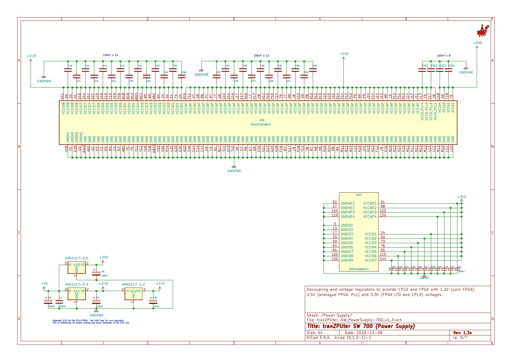
Using a larger FPGA device places a greater demand on decoupling, no less than 34 decoupling capacitors are deemed necessary by the Altera PDN tool. This made for interesting PCB placement and routing!
v1.3 Video Interface
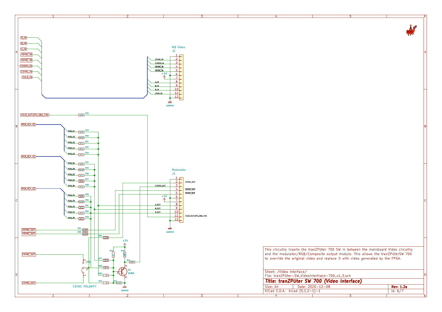
The video interface remains the same as v1.2.
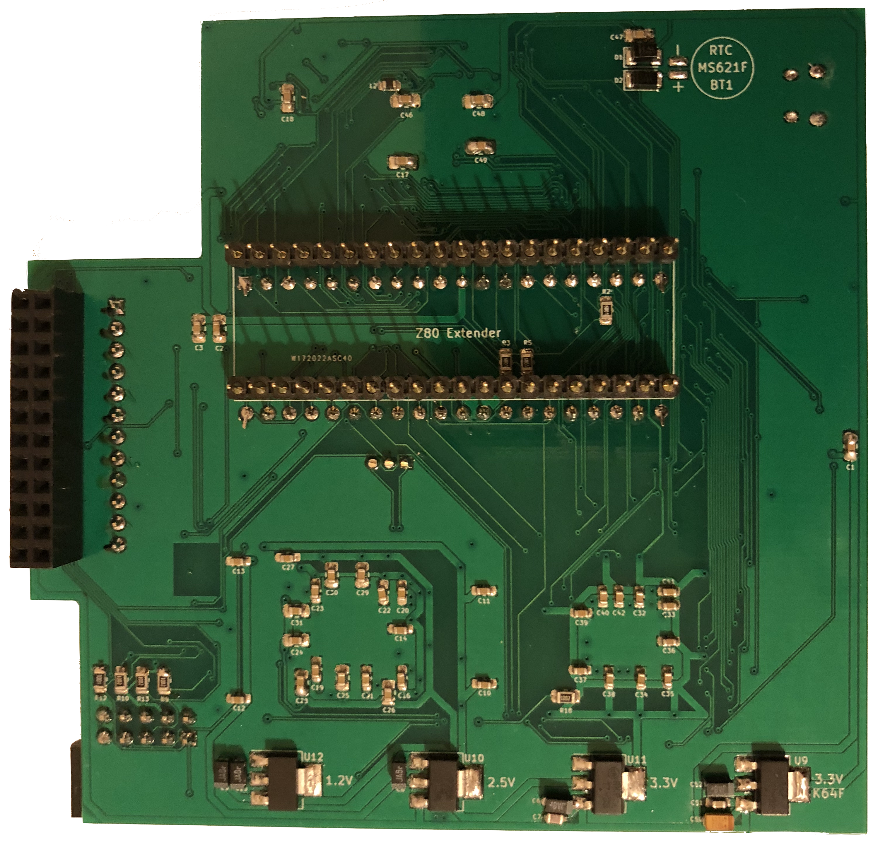
v1.3 PCB
Version 1.3 PCB is a rework of v1.2, replacing a 144 pin TQFP with a 484pin BGA, both identical in size but different in some parts placement and routing. The PCB remains as a 2 layer design but the inclusion of the BGA sees smaller via/land geometries and masked or filled via's. This increases the cost of PCB production several fold over the v1.2 design. The PCB had a routing error which given the production cost had to be reworked, involving BGA pad rerouting and drilling, an intricate process but one which wont be forgotten. The old adage, 'measure twice, cut once' comes to mind, I measured twice but didnt make a final check, more especially after a computer crash where I think the error originated, so my bad!
Design Detail
K64F Z80 Host API
// Structure to contain inter CPU communications memory for command service processing and results.
// Typically the z80 places a command into the structure in it's memory space and asserts an I/O request,
// the K64F detects the request and reads the lower portion of the struct from z80 memory space,
// determines the command and then either reads the remainder or writes to the remainder. This struct
// exists in both the z80 and K64F domains and data is sync'd between them as needed.
//
typedef struct __attribute__((__packed__)) {
    uint8_t                          cmd;                                // Command request.
    uint8_t                          result;                             // Result code. 0xFE - set by Z80, command available, 0xFE - set by K64F, command ack and processing. 0x00-0xF0 = cmd complete and result of processing.
    union {
        uint8_t                      dirSector;                          // Virtual directory sector number.
        uint8_t                      fileSector;                         // Sector within open file to read/write.
        uint8_t                      vDriveNo;                           // Virtual or physical SD card drive number.
    };
    union {
        struct {
            uint16_t                 trackNo;                            // For virtual drives with track and sector this is the track number
            uint16_t                 sectorNo;                           // For virtual drives with track and sector this is the sector number. NB For LBA access, this is 32bit and overwrites fileNo/fileType which arent used during raw SD access.
        };
        uint32_t                     sectorLBA;                          // For LBA access, this is 32bit and used during raw SD access.
    };
    uint8_t                          fileNo;                             // File number of a file within the last directory listing to open/update.
    uint8_t                          fileType;                           // Type of file being processed.
    union {
        uint16_t                     loadAddr;                           // Load address for ROM/File images which need to be dynamic.
        uint16_t                     saveAddr;                           // Save address for ROM/File images which need to be dynamic.
        uint16_t                     cpuFreq;                            // CPU Frequency in KHz - used for setting of the alternate CPU clock frequency.
    };
    union {
        uint16_t                     loadSize;                           // Size for ROM/File to be loaded.
        uint16_t                     saveSize;                           // Size for ROM/File to be saved.
    };
    uint8_t                          directory[TZSVC_DIRNAME_SIZE];      // Directory in which to look for a file. If no directory is given default to MZF.
    uint8_t                          filename[TZSVC_FILENAME_SIZE];      // File to open or create.
    uint8_t                          wildcard[TZSVC_WILDCARD_SIZE];      // A basic wildcard pattern match filter to be applied to a directory search.
    uint8_t                          sector[TZSVC_SECTOR_SIZE];          // Sector buffer generally for disk read/write.
} t_svcControl;
Communications are all instigated by the Z80. When it needs a service, it will write a command into the svcControl.cmd field and set the svcControl.result field to REQUEST. The Z80 then writes to an output port (configurable but generally 0x68) which in turn sends an interrupt to the K64F. The K64F reads the command and sets the svcControl.result to PROCESSING - the Z80 waits for this handshake, if it doesnt see it after a timeout period it will resend the command. The Z80 then waits for a valid result, again if it doesnt get a result in a reasonable time period it retries the sequence and after a number of attempts gives up with an error.
Once the K64F has processed the command (ie. read directory) and stored any necessary data into the structure, it sets the svcControl.result to a valid result (success, fail or error code) to complete the transaction.
API Command List
| Command | Cmd# | Description |
|---|---|---|
| TZSVC_CMD_READDIR | 0x01 | Open a directory and return the first block of entries. |
| TZSVC_CMD_NEXTDIR | 0x02 | Return the next block in an open directory. |
| TZSVC_CMD_READFILE | 0x03 | Open a file and return the first block. |
| TZSVC_CMD_NEXTREADFILE | 0x04 | Return the next block in an open file. |
| TZSVC_CMD_WRITEFILE | 0x05 | Create a file and save the first block. |
| TZSVC_CMD_NEXTWRITEFILE | 0x06 | Write the next block to the open file. |
| TZSVC_CMD_CLOSE | 0x07 | Close any open file or directory. |
| TZSVC_CMD_LOADFILE | 0x08 | Load a file directly into tranZPUter memory. |
| TZSVC_CMD_SAVEFILE | 0x09 | Save a file directly from tranZPUter memory. |
| TZSVC_CMD_ERASEFILE | 0x0a | Erase a file on the SD card. |
| TZSVC_CMD_CHANGEDIR | 0x0b | Change active directory on the SD card. |
| TZSVC_CMD_LOAD40ABIOS | 0x20 | Request 40 column version of the SA1510 BIOS to be loaded, change frequency to match the Sharp MZ-80A. |
| TZSVC_CMD_LOAD80ABIOS | 0x21 | Request 80 column version of the SA1510 BIOS to be loaded, change frequency to match the Sharp MZ-80A. |
| TZSVC_CMD_LOAD700BIOS40 | 0x22 | Request 40 column version of the 1Z-013A MZ-700 BIOS to be loaded, change frequency to match the Sharp MZ-700 and action memory page commands. |
| TZSVC_CMD_LOAD700BIOS80 | 0x23 | Request 80 column version of the 1Z-013A MZ-700 BIOS to be loaded, change frequency to match the Sharp MZ-700 and action memory page commands. |
| TZSVC_CMD_LOAD80BIPL | 0x24 | Request the loading of the MZ-80B IPL, switch frequency and enable Sharp MZ-80B compatible mode. |
| TZSVC_CMD_LOADBDOS | 0x30 | Reload CPM BDOS+CCP. |
| TZSVC_CMD_ADDSDDRIVE | 0x31 | Attach a CPM disk to a drive number. |
| TZSVC_CMD_READSDDRIVE | 0x32 | Read an attached SD file as a CPM disk drive. |
| TZSVC_CMD_WRITESDDRIVE | 0x33 | Write to a CPM disk drive which is an attached SD file. |
| TZSVC_CMD_CPU_BASEFREQ | 0x40 | Set the tranZPUter to use the mainboard frequency for the Z80. |
| TZSVC_CMD_CPU_ALTFREQ | 0x41 | Switch the Z80 to use the K64F generated clock, ie. alternative frequency. |
| TZSVC_CMD_CPU_CHGFREQ | 0x42 | Change the Z80 frequency generated by the K64F to the Hertz value given in svcControl.cpuFreq, the Z80 will be clocked at the nearest timer resolution of this frequency. |
| TZSVC_CMD_CPU_SETZ80 | 0x50 | Switch to the external Z80 hard cpu. |
| TZSVC_CMD_CPU_SETT80 | 0x51 | Switch to the internal T80 soft cpu. |
| TZSVC_CMD_CPU_SETZPUEVO | 0x52 | Switch to the internal ZPU Evolution cpu. |
| TZSVC_CMD_SD_DISKINIT | 0x60 | Initialise and provide raw access to the underlying SD card. |
| TZSVC_CMD_SD_READSECTOR | 0x61 | Provide raw read access to the underlying SD card. |
| TZSVC_CMD_SD_WRITESECTOR | 0x62 | Provide raw write access to the underlying SD card. |
| TZSVC_CMD_EXIT | 0x7F | Terminate TZFS and restart the machine in original mode. |
API Result List
| Command | Result# | Description |
|---|---|---|
| TZSVC_STATUS_OK | 0x00 | The K64F processing completed successfully. |
| TZSVC_STATUS_FILE_ERROR | 0x01 | A file or directory error. |
| TZSVC_STATUS_BAD_CMD | 0x02 | Bad service command was requested. |
| TZSVC_STATUS_BAD_REQ | 0x03 | Bad request was made, the service status request flag was not set. |
| TZSVC_STATUS_REQUEST | 0xFE | Z80 has posted a request. |
| TZSVC_STATUS_PROCESSING | 0xFF | K64F is processing a command. |
K64F GPIO Organisation
If advanced services are needed such as SD card access, alternate BIOS loading or variable alternative CPU clock then it needs the K64F to provide them, the Z80 see's the K64F as a hardware extension, it makes an I/O request and gets functionality in return.
If the Z80 for example requests a BIOS load, it generates an I/O out request which interrupts the K64F, the K64F puts the Z80 into tri-state bus mastered mode and then reads the BIOS from the SD card and operates the Z80 lines to write the BIOS data into the Z80 RAM.
In order to provide this functionality, the K64F needs to be able to read/write ALL of the Z80 signals. One of the advantages of the K64F is that it has an abundance of digitial I/O ports which are 5V tolerant, therefore connection and operation of a 5V Z80 system is relatively straight forward.
The pin allocation of Z80 signals to K64F GPIO Port/Pin is a little disjointed as the K64F doesnt have a linear allocation of GPIO pins to internal registers, ie. the GPIO pins are split over 5 32bit registers. This non-linear allocation adds overhead in piecing together 16bit address or 8bit data value's for realtime assembly and decode.
In earlier tranZPUter SW designs, the allocation of Z80 pins to GPIO Port/Pins led to some headaches in the interrupt service routine but these have now been solved by the addition of the CPLD which contains most of the time critical logic.
The following tables have been created to show Z80 signals to their associated K64F pins. The signals are spread across 5 x 32bit internal K64F registers.
K64F Port and Bit allocation
| BIT / PORT | 31 | 30 | 29 | 28 | 27 | 26 | 25 | 24 | 23 | 22 | 21 | 20 | 19 | 18 | 17 | 16 | 15 | 14 | 13 | 12 | 11 | 10 | 9 | 8 | 7 | 6 | 5 | 4 | 3 | 2 | 1 | 0 |
|---|---|---|---|---|---|---|---|---|---|---|---|---|---|---|---|---|---|---|---|---|---|---|---|---|---|---|---|---|---|---|---|---|
| A | Z80_NMI | Z80_INT | CTL_HALT | CTL_RFSH | CTL_M1 | SYSCLK | ||||||||||||||||||||||||||
| B | Z80_D7 | Z80_D6 | Z80_D5 | Z80_D4 | Z80_D3 | Z80_D2 | Z80_D1 | Z80_D0 | CTL_CLKSLCT | Z80_WAIT | Z80_MEM4 | Z80_MEM3 | Z80_MEM2 | Z80_MEM1 | Z80_MEM0 | |||||||||||||||||
| C | Z80_A16 | Z80_A17 | Z80_A18 | Z80_A15 | Z80_A14 | Z80_A13 | Z80_A12 | Z80_A11 | Z80_A10 | Z80_A9 | Z80_A8 | Z80_A7 | Z80_A6 | Z80_A5 | Z80_A4 | Z80_A3 | Z80_A2 | Z80_A1 | Z80_A0 | |||||||||||||
| D | Z80_RD | CTL_BUSACK | Z80_WR | Z80_RESET | Z80_IORQ | Z80_MREQ | CTL_CLK | CTL_BUSRQ | ||||||||||||||||||||||||
| E | Z80_BUSACK | SVCREQ |
GPIO bits to Z80 Address Line mapping
| ADDR 18 | ADDR 17 | ADDR 16 | ADDR 15 | ADDR 14 | ADDR 13 | ADDR 12 | ADDR 11 | ADDR 10 | ADDR 9 | ADDR 8 | ADDR 7 | ADDR 6 | ADDR 5 | ADDR 4 | ADDR 3 | ADDR 2 | ADDR 1 | ADDR 0 |
|---|---|---|---|---|---|---|---|---|---|---|---|---|---|---|---|---|---|---|
| PORT C:16 | PORT C:17 | PORT C:18 | PORT C:15 | PORT C:14 | PORT C:13 | PORT C:12 | PORT C:11 | PORT C:10 | PORT C:9 | PORT C:8 | PORT C:7 | PORT C:6 | PORT C:5 | PORT C:4 | PORT C:3 | PORT C:2 | PORT C:1 | PORT C:0 |
GPIO bits to Z80 Data Line mapping
| DATA 7 | DATA 6 | DATA 5 | DATA 4 | DATA 3 | DATA 2 | DATA 1 | DATA 0 |
|---|---|---|---|---|---|---|---|
| PORT B:23 | PORT B:22 | PORT B:21 | PORT B:20 | PORT B:19 | PORT B:18 | PORT B:17 | PORT B:16 |
Z80 Memory Modes
The basis of the memory modes came from version 1 of the tranZPUter SW project where the decoder was based on a Flash RAM. All foreseen memory models required at that time, such as MZ-700, CP/M etc where devised. These modes have been enhanced in later designs within the CPLD to cater for new features such as the Video Module and no doubt will be further enhanced in the future.
Modes which have been defined are in the table below leaving a few available slots for future expansion.
| Mode | Target | Range | Block | Function | DRAM Refresh | Description |
|---|---|---|---|---|---|---|
| 0 | Original | 0000:0FFF | Main | MROM | Yes | Default, normal host (ie. Sharp MZ80A/MZ-700) operating mode, all memory and IO (except tranZPUter controlled I/O block) are on the mainboard |
| 1000:CFFF | Main | D-RAM | ||||
| D000:D7FF | Main | VRAM | ||||
| D800:DFFF | Main | ARAM | ||||
| E000:E7FF | Main | MM I/O | ||||
| E800:EFFF | Main | User ROM | ||||
| F000:FFFF | Main | FDC ROM | ||||
| 1 | Orig+ UROM | 0000:0FFF | Main | MROM | Yes | As 0 except User ROM is mapped to tranZPUter RAM and used for loadable BIOS images. |
| 1000:CFFF | Main | D-RAM | ||||
| D000:D7FF | Main | VRAM | ||||
| D800:DFFF | Main | ARAM | ||||
| E000:E7FF | Main | MM I/O | ||||
| E800:EFFF | RAM 0 | User ROM | ||||
| F000:FFFF | Main | FDC ROM | ||||
| 2 | TZFS | 0000:0FFF | RAM 0 | MROM | No | Boot mode for TZFS or any other software requiring use of the tranZPUter RAM. User ROM appears as ROM to the Monitor so it will call the entry point at 0xE800 as part of it’s normal startup procedure. The software stored at 0xE800 can switch out the mainboard and run in tranZPUter RAM as required. Two small holes at F3FE and F7FE exist for the Floppy disk controller (which have to be 2 bytes wude), these locations need to be on the mainboard. The floppy disk controller uses them as part of its data read/write as the Z80 isnt fast enough to poll the FDC. |
| 1000:CFFF | RAM 0 | Main RAM | ||||
| D000:D7FF | Main | VRAM | ||||
| D800:DFFF | Main | ARAM | ||||
| E000:E7FF | RAM 0 | MM I/O | ||||
| E800:EFFF | RAM 0 | User ROM | ||||
| F000:FFFF | RAM 0 | FDC ROM | ||||
| 3 | TZFS | 0000:0FFF | RAM 0 | MROM | No | Page mode for TZFS, all RAM in tranZPUter Block 0 except F000:FFFF which is in Block 1, this is page bank2 of TZFS. |
| 1000:CFFF | RAM 0 | Main RAM | ||||
| D000:D7FF | RAM 0 | VRAM | ||||
| D800:DFFF | RAM 0 | ARAM | ||||
| E000:E7FF | RAM 0 | MM I/O | ||||
| E800:EFFF | RAM 0 | User ROM | ||||
| F000:FFFF | RAM 1 | FDC ROM | ||||
| 4 | TZFS | 0000:0FFF | RAM 0 | MROM | No | As mode 3 but F000:FFFF is in Block 2, this is page bank3 of TZFS. |
| 1000:CFFF | RAM 0 | Main RAM | ||||
| D000:D7FF | RAM 0 | VRAM | ||||
| D800:DFFF | RAM 0 | ARAM | ||||
| E000:E7FF | RAM 0 | MM I/O | ||||
| E800:EFFF | RAM 0 | User ROM | ||||
| F000:FFFF | RAM 2 | FDC ROM | ||||
| 5 | TZFS | 0000:0FFF | RAM 0 | MROM | No | As mode 3 but F000:FFFF is in Block 3, this is page bank4 of TZFS. |
| 1000:CFFF | RAM 0 | Main RAM | ||||
| D000:D7FF | RAM 0 | VRAM | ||||
| D800:DFFF | RAM 0 | ARAM | ||||
| E000:E7FF | RAM 0 | MM I/O | ||||
| E800:EFFF | RAM 0 | User ROM | ||||
| F000:FFFF | RAM 3 | FDC ROM | ||||
| 6 | CP/M | 0000:FFFF | RAM 4 | Main RAM | No | CP/M, all memory on the tranZPUter board. Special case for F3C0:F3FF & F7C0:F7FF (floppy disk paging vectors) which resides on the mainboard. |
| 7 | CP/M | 0000:0100 | RAM 4 | CP/M Vectors | No | CP/M main CBIOS area, 48K + 2K available for the CBIOS and direct access to mainboard hardware. F000:FFFF remains in bank 4 and used as the gateway between this memory mode and mode 6. |
| 0100:CFFF | RAM 5 | Main RAM | ||||
| D000:D7FF | Main | VRAM | ||||
| D800:DFFF | Main | ARAM | ||||
| E000:E7FF | Main | MM I/O | ||||
| E800:EFFF | RAM 5 | User ROM | ||||
| F000:FFFF | RAM 4 | FDC ROM | ||||
| 8 | Orig+ Emu | 0000:0FFF | Main | MROM | Yes | Original mode but with the main RAM in the tranZPUter bank 0. This mode is used to bootstrap programs such as MZ-700 programs which bank change on startup and expect the loaded program to be within the main memory which is within a tranZPUter RAM bank. |
| 1000:CFFF | RAM 0 | Main RAM | ||||
| D000:D7FF | Main | VRAM | ||||
| D800:DFFF | Main | ARAM | ||||
| E000:E7FF | Main | MM I/O | ||||
| E800:EFFF | Main | User ROM | ||||
| F000:FFFF | Main | FDC ROM | ||||
| 10 | MZ-700 | 0000:0FFF | RAM 6 | Main RAM | No | MZ-700 mode (OUT $E0) - Monitor RAM replaced with Main RAM |
| 1000:CFFF | RAM 0 | Main RAM | ||||
| D000:D7FF | Main | VRAM | ||||
| D800:DFFF | Main | ARAM | ||||
| E000:E7FF | Main | MM I/O | ||||
| E800:EFFF | Main | User ROM | ||||
| F000:FFFF | Main | FDC ROM | ||||
| 11 | MZ-700 | 0000:0FFF | RAM 0 | MROM | No | MZ-700 mode (OUT $E0 + $E1) - I/O and Video block replaced with Main RAM |
| 1000:CFFF | RAM 0 | Main RAM | ||||
| D000:D7FF | RAM 6 | VRAM | ||||
| D800:DFFF | RAM 6 | ARAM | ||||
| E000:E7FF | RAM 6 | MM I/O | ||||
| E800:EFFF | RAM 6 | User ROM | ||||
| F000:FFFF | RAM 6 | FDC ROM | ||||
| 12 | MZ-700 | 0000:0FFF | RAM 6 | Main RAM | No | MZ-700 mode (OUT $E1 + $E2) - Monitor RAM replaced with RAM and I/O and Video block replaced with Main RAM |
| 1000:CFFF | RAM 0 | Main RAM | ||||
| D000:D7FF | RAM 6 | VRAM | ||||
| D800:DFFF | RAM 6 | ARAM | ||||
| E000:E7FF | RAM 6 | MM I/O | ||||
| E800:EFFF | RAM 6 | User ROM | ||||
| F000:FFFF | RAM 6 | FDC ROM | ||||
| 13 | MZ-700 | 0000:0FFF | RAM 0 | MROM | No | MZ-700 mode (OUT $E5) - Upper memory locked out, Monitor ROM paged in. |
| 1000:CFFF | RAM 0 | Main RAM | ||||
| D000:FFFF | n/a | Undefined | ||||
| 14 | MZ-700 | 0000:0FFF | RAM 6 | Main RAM | No | MZ-700 mode (OUT $E6) - Monitor RAM replaced with RAM and Upper memory locked out. |
| 1000:CFFF | RAM 0 | Main RAM | ||||
| D000:FFFF | n/a | Undefined | ||||
| 15 | MZ-800/MZ-700 | See table below. Memory mode is as per the MZ-800. | ||||
| 21 | K64F Access | 000000:FFFFFF | n/a | FPGA Resources | No | Access the FPGA memory by passing through the full 24bit Z80 address, typically from the K64F. |
| 22 | FPGA Access | 0000:FFFF | n/a | Host Resources | Yes | Access to the host mainboard 64K address space only. |
| 23 | K64F Access | 000000:FFFFFF | RAM | Main RAM | No | Access all memory and IO on the tranZPUter board with the K64F addressing the full 512K RAM. |
| 24 | K64F Access | 0000:FFFF | RAM 0 | Main RAM | Yes/No | All memory and IO are on the tranZPUter board, 64K block 0 selected. Mainboard DRAM is refreshed by the tranZPUter library when using this mode. |
| 25 | K64F Access | 0000:FFFF | RAM 1 | Main RAM | Yes/No | All memory and IO are on the tranZPUter board, 64K block 1 selected. Mainboard DRAM is refreshed by the tranZPUter library when using this mode. |
| 26 | K64F Access | 0000:FFFF | RAM 2 | Main RAM | Yes/No | All memory and IO are on the tranZPUter board, 64K block 2 selected. Mainboard DRAM is refreshed by the tranZPUter library when using this mode. |
| 27 | K64F Access | 0000:FFFF | RAM 3 | Main RAM | Yes/No | All memory and IO are on the tranZPUter board, 64K block 3 selected. Mainboard DRAM is refreshed by the tranZPUter library when using this mode. |
| 28 | K64F Access | 0000:FFFF | RAM 4 | Main RAM | Yes/No | All memory and IO are on the tranZPUter board, 64K block 4 selected. Mainboard DRAM is refreshed by the tranZPUter library when using this mode. |
| 29 | K64F Access | 0000:FFFF | RAM 5 | Main RAM | Yes/No | All memory and IO are on the tranZPUter board, 64K block 5 selected. Mainboard DRAM is refreshed by the tranZPUter library when using this mode. |
| 30 | K64F Access | 0000:FFFF | RAM 6 | Main RAM | Yes/No | All memory and IO are on the tranZPUter board, 64K block 6 selected. Mainboard DRAM is refreshed by the tranZPUter library when using this mode. |
| 31 | K64F Access | 0000:FFFF | RAM 7 | Main RAM | Yes/No | All memory and IO are on the tranZPUter board, 64K block 7 selected. Mainboard DRAM is refreshed by the tranZPUter library when using this mode. |
MROM = Monitor ROM, the original boot firmware ie. SA-1510
D-RAM = Dynamic RAM on the mainboard.
VRAM = Video RAM on the mainboard.
ARAM = Colour Attribute RAM on the mainboard.
MM I/O = Memory Mapped I/O controllers on the mainboard.
RAM 0 .. 7 = 64K RAM Block number within the 512K Static RAM chip.
Main = Host computer mainboard, ie the Sharp MZ-80A mainboard.
MZ700/MZ800 Memory Mode
| MZ-700 | MZ-800 | |||||||||||
|---|---|---|---|---|---|---|---|---|---|---|---|---|
| Register | 0000:0FFF | 1000:1FFF | 1000:CFFF | C000:CFFF | D000:FFFF | 0000:7FFF | 1000:1FFF | 2000:7FFF | 8000:BFFF | C000:CFFF | C000:DFFF | E000:FFFF |
| OUT 0xE0 | DRAM | DRAM | ||||||||||
| OUT 0xE1 | DRAM | DRAM | ||||||||||
| OUT 0xE2 | MONITOR | MONITOR | ||||||||||
| OUT 0xE3 | Memory Mapped I/O | Upper MONITOR ROM | ||||||||||
| OUT 0xE4 | MONITOR | DRAM | Memory Mapped I/O | MONITOR | CGROM | DRAM | VRAM | DRAM | Upper MONITOR ROM | |||
| OUT 0xE5 | Inhibit | Inhibit | ||||||||||
| OUT 0xE6 | ||||||||||||
| IN 0xE0 | CGROM* | VRAM* | CGROM | VRAM | ||||||||
| IN 0xE1 | DRAM | DRAM | DRAM |
<return> = Return to the state prior to the complimentary command being invoked.
* = MZ-800 host only.
Z80 CPU Frequency Switching
One of the main issues with frequency switching is that the underlying host cannot have its frequency changed, the host is generally generating the clock and it's circuits have been designed to operate within it's clock tolerances. The tranZPUter SW-700 overcomes this limitation as described below.
To fulfil the requirement to have a switchable Z80 CPU frequency a positive edge triggered frequency switch has been implemented which takes the host frequency as one input and a square wave generator from the K64F as its second input. The switching mechanism is tied to the bus control logic and so any access to the host will see the frequency of the CPU being changed to that of the host which ensures continued reliable operation. Under startup conditions, the Z80 is always clocked by the host clock to ensure original specifications of the machine are met.
A second frequency can be selected if the K64F is present as it has the ability using its onboard timers to generate a programmable square wave output. The K64F sets the frequency of this second clock source and the Z80 can select it via an I/O OUT command. This gives the software running on the Z80 the opportunity to change it's own frequency, albeit to a fixed set one. An extension to the K64F Host API allows the Z80 to make a request of the K64F to set the Z80 CPU frequency to any possible value, this is useful in TZFS or CP/M so a user can select their own frequency.
Current testing on a CMOS Z84C0020 20MHz CPU has the following observations:
- tranZPUter reliable in the range 1Hz to 24MHz for all functionality.
- When the mainboard is accessed the frequency slows to 3.54MHz (ie. the system clock) and returns to the higher frequency after the mainboard access has completed.
It is also possible to slow down the CPU for training or debugging purposes albeit access to the host circuitry will always run at the host clock frequency,
On an application running under the Z80, the following table outlines the I/O ports to which it must read/write in order to switch frequencies.
Z80 CPU Frequency Switching Ports
| Port | Dir | Function |
|---|---|---|
| 0x62 | W | Switch Z80 CPU frequency to the second source, ie. the frequency generated by the K64F or external oscillator. |
| 0x64 | W | Switch Z80 CPU frequency to default host source. This is the default on RESET. |
| 0x66 | R | Bit [0] - Clock Selected, 0 = Host Clock, 1 = second clock source (K64F or external oscillator). |
System Configuration
The CPLD holds an internal configuration register to change how it operates with the underlying host. The table below outlines the ports along with each bits function.
System Configuration Register (0x6E - 110 decimal)
| Bits | Dir | Description |
|---|---|---|
| 2:0 | R/W | Set hardware model compatibility. This configures the CPLD to remap host hardware to be compatible with the configured model. 000 = MZ-80K 001 = MZ-80C 010 = MZ-1200 011 = MZ-80A 100 = MZ-700 101 = MZ-800 110 = MZ-80B 111 = MZ-2000 |
| 3 | R/W | Set the mainboard video state, 0 = enabled, 1 = disabled. If the mainboard video is enabled, the FPGA enhanced video will be disabled. |
| 4 | R/W | Set the video wait state generator to be used during FPGA Video frame rendering, 0 = wait state disabled, 1 = enabled. |
| 7 | R/W | Preserve configuration over reset (=1) or set to default on reset (=0). |
NB: The compatibility modes which have been implemented appear in the paragraphs below, all other modes are yet to be implemented. Selecting a mode which hasnt been implemented results in no mapping and reverts to the base MZ-700 hardware.
The CPLD also holds a read only information register which indicates the capabilities of the running machine.
System Information Register (0x6F - 111 decimal)
| Bits | Dir | Description |
|---|---|---|
| 2:0 | R | The underlying host model in which the tranZPUter is installed, ie. the physical computer hardware. 000 = MZ-80K 001 = MZ-80C 010 = MZ-1200 011 = MZ-80A 100 = MZ-700 101 = MZ-800 110 = MZ-80B 111 = MZ-2000 |
| 3 | R | FPGA Video Module installed, 0 = not installed, 1 = installed. |
| 7:5 | R | Version number of the CPLD. Used by Z80 code when newer versions of the CPLD VHDL provide differing features. |
Soft Processors
In the FPGA or even ASIC world, the word 'soft' can often be used out of context. A 'soft' processor isnt a software emulation, it is a physical hardware device described in a HDL which can be instantiated and used inside an FPGA or masked onto an ASIC. The 'soft' is more relevant to FPGA where you can change the actual hardware device by uploading a new interconnect map at will. This is because an FPGA (Field Programmable Gate Array) is a mass of electronic components with an interconnect layer and this interconnect layer is like RAM where a '1' will link two components together. You load up an interconnect bit map either by a JTAG programming tool or via one of the FPGA's supported protocols such as a serial Flash configuration device. Once a device is instantiated and its interconnect loaded, it behaves like any other piece of hardware and so a 'soft' processor in an FPGA, when running, is the same as any other 'hard' processor.
Initially, to work out the framework for a 'soft' CPU to exist in the FPGA yet control the underlying Sharp MZ-700 hardware I chose to embed a T80 processor. This is a redesign of the venerable Zilog Z80 and achieves near cycle accuracy implementing all the documented and undocumented instructions and presenting the correct hardware signals for external use. The design required changes in the CPLD as it now had to be a bidirectional gateway along with instantiation of a T80 processor and support logic within the FPGA. The end result was a processor, running in the FPGA on a Sharp MZ-700 which was identical to the 'hard' Z80 running on the tranZPUter card.
Apart from aiding in the framework design, the 'soft' T80 has no advantages over a 'hard' Z80 except that you can modify the architecture/instructions for research or to aid a program speed and optionally choose the enhanced 'fast' mode of the T80. The actual Fmax is slower than the 'hard' Z80 due to the switching and propogation delays of the FPGA/CPLD, the 'hard' Z80 can run at 24MHZ, the T80 tops out at 18MHz. NB. If RAM was instantiated on the FPGA and the T80 ran from FPGA BRAM instead of the hard 512K static RAM on the tranZPUter card it would achieve speeds upto 120MHz as it does in my Sharp MZ Series Emulator but this would require reworking of the control software (TZFS and the 1Z-013A monitor) as the memory model would be different.
Keeping with the Z80 theme, the AZ80 and the NextZ80 were added as build time choices (instead of the T80) for evaluation and comparison. The AZ80 has some slight I/O timing issues which result in an odd spurious keyboard read but otherwise runs flawlessly with all the MZ-700 software I tested. The NextZ80 is more of an instruction compatible Z80 processor and doesnt present all the correct signals or follow the Z80 timing cycles, so more work is needed to make it run correctly.
The second processor added is the ZPU Evolution, a 32bit stack based processor originally written by Øyvind Harboe from Zylin AS as a minimal logic size CPU to run in a supervisory mode in embedded systems. There have been a few extensions to the design, the ZPU Flex and ZPUINO of note, but both didnt offer what I wanted for embedding into the Sharp MZ Series Emulator, so I redesigned it to gain speed and expandability creating the ZPU Evolution.
As the ZPU Evolution was intended to be embedded, zOS was written with this functionality in mind, an OS which would run tasks inside a device to enhance it’s functionality along with provision of an interactive session over a serial connection. Using a console connected to the serial connection you would be presented with an MS-DOS like environment where you could run applications, control hardware or inspect/update memory and process flow, an ideal tool to work with a ‘soft’ ZPU Evolution running inside an FPGA which in turn was running inside an end application such as the Sharp MZ Series Emulator. When the tranZPUter SW project was born, zOS was ported to the K64F which has been a great asset, being able to connect inside the tranZPUter SW and the Sharp MZ host has aided design and debug immensely.
Adding a ZPU Evo into the tranZPUter SW-700 as a ‘soft’ processor required zOS to evolve, it no longer had serial connectivity and was required to control keyboard, screen etc directly. This led to the SharpMZ module being added which provides zOS with the basic hardware abstraction layers to drive the Sharp MZ-700 keyboard and screen, providing the basic user I/O functionality including an ANSI terminal emulator. When the ZPU is selected from the Sharp MZ-700 monitor, zOS boots and you are presented with an interactive, MS-DOS like environment. There are some basic applications such as tbasic, mbasic. kilo (a VT100 based screen editor) and these can all be found in the apps section of zOS. As can be imagined, there isnt a lot of software to be run under zOS, although a lot of open source projects can be ported, the limiting factor is the GNU C/C++ 99 standard compiler or missing features such as thread control and virtual memory.
I am currently looking at instantiating a NIOSII processor with MMU as the FPGA has the resources to implement this processor and its support circuits and the end result would be Linux running on a Sharp MZ-700. This would be a far more useful platform so consider this is work in progress until completed and this page updated.
CPU Configuration Registers
CPU Configuration Register (0x6C - 108 decimal)
| Bits | Dir | Description |
|---|---|---|
| 5:0 | R/W | This register configures the FPGA to enable a soft/hard CPU and the CPLD is reconfigured to allow a CPU operation on the FPGA side rather than the physical hardware side. Only one processor can be selected at one time, 1 bit per processor. Multiple bit selection will be voided and the hard processor selected. 000000 = Hard CPU 000001 = T80 CPU 000010 = ZPU Evolution 000100 = NIOS11 001000 = Future CPU 4 010000 = Future CPU 5 100000 = Future CPU 6 |
| 6 | R/W | Clock enable. Enable (1) or disable the soft CPU clock. |
| 7 | R/W | CPU Reset. When set to active (‘1’), a reset pulse is generated and the bit state returned to 0. |
The FPGA holds a read only information register which indicates the soft processor capabilities.
CPU Information Register (0x6D - 109 decimal)
| Bits | Dir | Description |
|---|---|---|
| 5:0 | R | Bit mask, a 1 indicates a processor is available. 000000 = Hard CPU only 000001 = T80 CPU 000010 = ZPU Evolution 000100 = NIOSII 001000 = Future CPU 4 010000 = Future CPU 5 100000 = Future CPU 6 |
| 7:6 | R | Soft CPU capabilities, 01 = soft cpu capable, all other values indicate soft cpu capabilities not available. |
ZPU Memory Map.
The ZPU has a configurable linear address space, typically 18-32 bit wide. When used as a soft processor it is configured for 24bit.
| Address Range | Sub Range | Description |
|---|---|---|
| 000000:020000 | 000000:013FFF | zOS Kernel. |
| 014000:01BFFF | Heap. | |
| 01C000:01FD7F | Stack. | |
| 01FD80:01FFFF | I/O processor service control record. Used for inter processor communications between the ZPU and the K64F so that the ZPU can make service calls, ie. read SD card. | |
| 100000:180000 | 512Kbyte 8bit wide static RAM on tranZPUter board. Applications are loaded and run from this area of RAM starting at 0x100000. | |
| D00000:EFFFFF | Z80 Bus State Machine. Depending on the accessed address will determine the type of transaction. In order to provide byte level access on a 32bit read CPU, a bank of addresses, word aligned per byte is assigned in addition to an address to read 32bit word aligned value. | |
| D00000:D7FFFF | 512K Static RAM on the tranZPUter board. All reads are 32bit, all writes are 8, 16 or 32bit wide on word boundary. | |
| D80000:DBFFFF | 64K address space on host mainboard (ie. RAM/ROM/Memory mapped I/O) accessed 1 byte at a time. The physical address is word aligned per byte, so 4 bytes on the ZPU address space = 1byte on the Z80 address space. ie. 0x00780 ZPU = 0x0078 Z80. | |
| DC0000:DFFFFF | 64K I/O space on the host mainboard or the underlying CPLD/FPGA. 64K address space is due to the Z80 ability to address 64K via the Accumulator being set in 15:8 and the port in 7:0. The ZPU, via a direct address will mimic this ability for hardware which requires it. ie. A write to 0x3F with 0x10 in the accumulator would yield an address of 0xF103f. All reads are 8 bit, writes are 8, 16 or 32bit wide on word boundary. The physical address is word aligned per byte, so 4 bytes on the ZPU address space = 1byte on the Z80 address space. ie. 0x00780 ZPU = 0x0078 Z80. | |
| E00000:E0FFFF | 64K address space on host mainboard (ie. RAM/ROM/Memory mapped I/O) accessed 4 bytes at a time, a 32 bit read will return 4 consecutive bytes, start of read must be on a 32bit word boundary. | |
| E80000:EFFFFF | 512K Video address space - the video processor memory is directly mapped into ZPU memory address space. See the Video controller direct access mode below for a detailed explanation. | |
| E80000:E8FFFF | 64K Video / Attribute RAM | |
| E90000:E9FFFF | 64K Character Generator ROM/PCG RAM. | |
| EA0000:EBFFFF | 128K Red Framebuffer address space. | |
| EC0000:EDFFFF | 128K Blue Framebuffer address space. | |
| EE0000:EFFFFF | 128K Green Framebuffer address space. | |
| F00000:FFFFFF | F00800:F008FF | Interrupt Controller. Spacing between interrupt controller devices = 0x10. |
| F00800:F00803 | Status Register. | |
| F00804:F00807 | Control Register. | |
| F00900:F009FF | SD Card Controller. | |
| F00900:F00903 | Address Register. | |
| F00904:F00907 | Data Register. | |
| F0090c:F0090f | Status Register. | |
| F00C00:F00CFF | Timer. Spacing between timer devices = 0x40. | |
| F00C00:F00C3F | Timer 0. | |
| F00C00:F00C03 | TIMER_MICROSEC_DOWN - Programmable microsecond down counter. | |
| F00C04:F00C07 | TIMER_MILLISEC_DOWN - Programmable millisecond down counter. | |
| F00C08:F00C0B | TIMER_MILLISEC_UP - Programmable millisecond up counter. | |
| F00C0C:F00C0F | TIMER_SECONDS_DOWN - Programmable second down counter. | |
| F00C1C:F00C1F | RTC_MILLISECONDS_EPOCH - Real Time milliseconds since EPOCH. | |
| F00C20:F00C23 | RTC_MICROSECONDS - Real Time microseconds count in current second. | |
| F00C24:F00C27 | RTC_MILLISECONDS - Real Time milliseconds count in current second. | |
| F00C28:F00C2B | RTC_SECOND - Real Time seconds count. | |
| F00C2C:F00C2F | RTC_MINUTE - Real Time minutes count. | |
| F00C30:F00C33 | RTC_HOUR - Real Time hours count. | |
| F00C34:F00C37 | RTC_DAY - Real Time days in month count. | |
| F00C38:F00C3B | RTC_MONTH - Real Time month in year count. | |
| F00C3C:F00C3F | RTC_YEAR - Real Time current year count. | |
| F00C40:F00C7F | Timer 1 .. n, hardware build dependent. | |
| F00C40:F00C43 | Enable Register. | |
| F00C44:F00C47 | Index Register. | |
| F00C48:F00C4b | Counter Register. | |
| F00F00:F00FFF | System on Chip Configuration. | |
| F00F00:F00F03 | SOCCFG_ZPU_ID - ID of the instantiated ZPU | |
| F00F04:F00F07 | SOCCFG_SYSFREQ - System Clock Frequency in MHz x 10 (ie. 100MHz = 1000) | |
| F00F08:F00F0B | SOCCFG_MEMFREQ - Sysbus SDRAM Clock Frequency in MHz x 10 (ie. 100MHz = 1000) | |
| F00F0C:F00F0F | SOCCFG_WBMEMFREQ - Wishbone SDRAM Clock Frequency in MHz x 10 (ie. 100MHz = 1000) | |
| F00F00:F00F03 | SOCCFG_DEVIMPL - Bit map of devices implemented in SOC. | |
| F00F04:F00F07 | SOCCFG_BRAMADDR - Address of Block RAM. | |
| F00F08:F00F0B | SOCCFG_BRAMSIZE - Size of Block RAM. | |
| F00F0C:F00F0F | SOCCFG_RAMADDR - Address of RAM (additional BRAM, DRAM etc). | |
| F00F00:F00F03 | SOCCFG_RAMSIZE - Size of RAM. | |
| F00F04:F00F07 | SOCCFG_BRAMINSNADDR - Address of dedicated instruction Block RAM. | |
| F00F08:F00F0B | SOCCFG_BRAMINSNSIZE - Size of dedicated instruction Block RAM. | |
| F00F0C:F00F0F | SOCCFG_SDRAMADDR - Address of SDRAM. | |
| F00F00:F00F03 | SOCCFG_SDRAMSIZE - Size of SDRAM. | |
| F00F04:F00F07 | SOCCFG_WBSDRAMADDR - Address of Wishbone SDRAM. | |
| F00F08:F00F0B | SOCCFG_WBSDRAMSIZE - Size of Wishbone SDRAM. | |
| F00F0C:F00F0F | SOCCFG_CPURSTADDR - Address CPU executes after a RESET. | |
| F00F00:F00F03 | SOCCFG_CPUMEMSTART - Start address of Memory containing BIOS/Microcode for CPU. | |
| F00F04:F00F07 | SOCCFG_STACKSTART - Start address of Memory for Stack use. |
Video Module
Using the FPGA allows the tranZPUter SW-700 to provide video capabilites for nearly all the Sharp MZ series, ie: MZ-80K, MZ-80C, MZ-1200, MZ-80A, MZ-700, MZ-80B (including graphics). In the near future the video capabilities will be upgraded to include the MZ-800 and MZ-2000 machines. To use a specific machines video capabilities, a mode (described below) is written into the mode register to select the required video capabilites based on machine model and you then use the normal methods of accessing the video of the selected machine ie. 0xD000-0xD7FF for video on an MZ-80A. This includes functions such as the invert or hardware scroll functionality.
An addition to the original Sharp MZ series capabilites, is the addition of a 640x200/320x200 8 colour Graphics frame buffer. This frame buffer is made up of 3x16K RAM blocks, 1 per colour with a resolution of 640x200 which matches the output display buffer bit for bit. If the display is working at 40x25 characters then the resolution is 320x200, otherwise for 80x25 it is 640x200.
For all modes except 640x200 (limitation only the Cyclone III) the display is double buffered whereby the image is assembled in a seperate buffer to the one which is rendered for screen display. Due to lack of memory in the Cyclone III FPGA, in 640x200 mode the display isnt double buffered and therefore an optional WAIT state generator can be enabled to prevent screen snow/tear as required. The Cyclone IV has sufficient RAM to double buffer, as per the Sharp MZ Series Emulator from where the video logic design was taken.
The RAM for the Graphics frame buffer can be switched into the main CPU address range C000H – FFFFH by programmable registers, 1 bank at a time (ie. Red, Green, Blue banks). This allows for direct CPU addressable pixels to be read and/or written. Each pixel is stored in groups of 8 (1 byte in RAM) scanning from right to left per byte, left to right per row, top to bottom. Ie. if the Red bank is mapped into CPU address space, the byte at C000H represents red pixels 7 - 0 of 320/640 (X) at pixel 0 of 200 (Y). Thus 01H written to C000H would set Pixel 7 (X), Row 0 (Y) to On, 80H written to C000H would set pixel 0 (X), Row 0 (Y) . This applies for Green and Blue banks when mapped into CPU address space.
In order to speed up the display, there is a Colour Write register (similar to what is available on the Sharp MZ-2500), so that a write to the graphics RAM will update all 3 banks at the same time which allows for immediate colour write.
Programmable Registers
In order to make use of the video functionality a set of registers have been designed through which all functions can be accessed.
The functionality is grouped as follows:
- Control - set the video capability mode, set the column width, set the colour/mono capabilities.
- Graphics - configure the graphics capability.
- GPU - offload tasks to the inbuilt graphics processor to speed up video tasks.
- Palette - set and configure the display palette.
The registers lie in the upper I/O region from 0xD0 - 0XFD and are accessed with standard Z80 I/O commands IN/OUT. Unless otherwise stated, all registers are read/write and a read will return the current value stored.
Control Register (0xF8 - 248 decimal)
This is the video mode register. It specifies the hardware model the Video Module should function as in addition the column width and colour abilities of the output display.
| Bits | Dir | Description |
|---|---|---|
| 2:0 | R/W | Set the hardware model of the Video Module. 000 = MZ-80K 001 = MZ-80C 010 = MZ-1200 011 = MZ-80A 100 = MZ-700 101 = MZ-800 110 = MZ-80B 111 = MZ-2000 |
| 3 | R/W | Set the column width of the video output. 0 = 40 Column, 1 = 80 Column |
| 4 | R/W | Set the colour capabilities of the video output. 0 = Monochrome, 1 = Colour. |
| 5 | R/W | Enable the Programmable Character Generator RAM. 0 = disabled, 1 = enabled. |
| 7:6 | R/W | Set the VGA mode. 00 = Original MZ video format, 15.62KHz Horizontal x 60Hz Vertical. 01 = VGA 640x480 @ 60Hz 10 = VGA 1024x768 @ 60Hz 11 = VGA 800x600 @ 60Hz. |
Graphics Mode Register (0xF9 - 249 decimal)
This is the graphics mode control register. It specifies what video is to be output, how it is blended and which Graphics RAM bank can be read/written to.
| Bits | Dir | Description |
|---|---|---|
| 1:0 | R/W | Read mode (00=Red Bank, 01=Green Bank, 10=Blue Bank, 11=Not used). Select which bank to be read when enabled in CPU address space. |
| 3:2 | R/W | Write mode (00=Red Bank, 01=Green Bank, 10=Blue Bank, 11=Indirect). Select which bank to be written to when enabled in CPU address space. |
| 4 | R/W | VRAM Output. 0=Enable, 1=Disable. Output Character RAM to the display. |
| 5 | R/W | GRAM Output. 0=Enable, 1=Disable. Output Graphics RAM to the display. |
| 7:6 | R/W | Blend Operator (00=OR ,01=AND, 10=NAND, 11=XOR). Operator to blend Character display with Graphics Display. |
Colour Writer Registers (0xFA - 250 decimal to 0xFC - 252 decimal)
For Indirect mode (Control Register bits 3/2 set to 11), a write to the Graphics RAM when mapped into CPU address space C000H – FFFFH will see the byte masked by the Red Colour Writer Register and written to the Red Bank with the same operation for Green and Blue. This allows rapid setting of a colour across the 3 banks.
ie. Red Filter = 0x80, Green Filter = 0x40, Blue Filter = 0x20, then an indirect write to address C000H will set pixel 0,0 to red, 1,0 to green, 2,0 to blue.
| Bit | Dir | Pixel | I/O Addr | Colour | Description |
|---|---|---|---|---|---|
| 0 | R/W | 7 | 0xFAH | Red | Set to Red during indirect write. |
| 1 | R/W | 6 | 0xFAH | Red | |
| 2 | R/W | 5 | 0xFAH | Red | |
| 3 | R/W | 4 | 0xFAH | Red | |
| 4 | R/W | 3 | 0xFAH | Red | |
| 5 | R/W | 2 | 0xFAH | Red | |
| 6 | R/W | 1 | 0xFAH | Red | |
| 7 | R/W | 0 | 0xFAH | Red | Set to Red during indirect write. |
| 0 | R/W | 7 | 0xFBH | Green | Set to Green during indirect write. |
| 1 | R/W | 6 | 0xFBH | Green | |
| 2 | R/W | 5 | 0xFBH | Green | |
| 3 | R/W | 4 | 0xFBH | Green | |
| 4 | R/W | 3 | 0xFBH | Green | |
| 5 | R/W | 2 | 0xFBH | Green | |
| 6 | R/W | 1 | 0xFBH | Green | |
| 7 | R/W | 0 | 0xFBH | Green | Set to Green during indirect write. |
| 0 | R/W | 7 | 0xFCH | Blue | Set to Blue during indirect write. |
| 1 | R/W | 6 | 0xFCH | Blue | |
| 2 | R/W | 5 | 0xFCH | Blue | |
| 3 | R/W | 4 | 0xFCH | Blue | |
| 4 | R/W | 3 | 0xFCH | Blue | |
| 5 | R/W | 2 | 0xFCH | Blue | |
| 6 | R/W | 1 | 0xFCH | Blue | |
| 7 | R/W | 0 | 0xFCH | Blue | Set to Blue during indirect write. |
Memory Page Registers (0xFD - 253 decimal)
This register is responsible for enabling Video memory into Z80 address space. It is possible to enable 1 of the 3 colour 16KB GRAM (chosen via the Graphics Mode register) into Z80 address C000:FFFF or the CGROM into Z80 address space D000:DFFF. This register overrides all other memory page settings.
| Bits | Dir | Description |
|---|---|---|
| 0 | R/W | Switches in a 16Kb graphics ram bank to C000 - FFFF. The bank (or colour) is selected by the Graphics Mode register. 0 = Off, normal Z80 memory operations. 1 = 16KB GRAM enabled. Setting this register overrides all MZ-700/MZ-80B specific memory page settings. |
| 7 | R/W | Switches in CGROM for upload at D000:DFFF. 0 - Normal memory operations, 1 - CGROM paged in. |
Video Module Status Register (0xFD - 253 decimal)
This register reports on the Video Module status. Bits 7 & 0 are reserved for reporting the Memory Page register settings.
| Bits | Dir | Description |
|---|---|---|
| 5 | R | Framebuffer Horizontal Blanking. 1 = Horizontal Blanking active, 0 = no horizontal blanking. |
| 6 | R | Framebuffer Vertical Blanking. 1 = Vertical Blanking active, 0 = no vertical blanking. |
GPU Parameters Register (0xF6 - 246 decimal)
A read from this register pops off bits 7:0 then shifts the register right by 8 bits.
GPU Command Register (0xF7 - 247 decimal)
| Command | Parameters | Description |
|---|---|---|
| 0x00 | n/a | No operation. This is the idle state command when the GPU isnt busy, issuing it performs no action. |
| 0x01 | n/a | Clear VRAM screen. The entire video and attribute RAM are cleared to space character (ie. blank) with white characters on a blue background. |
| 0x02 | [15:8] - character [7:0] - attribute byte |
Clear VRAM screen with char and attribute. The entire video and attribute RAM are cleared to the values given in the parameter list. |
| 0x03 | [47:40] - Start X [39:32] - Start Y [31:24] - End X [23:16] - End Y [15:8] - display char [7:0] - attribute byte. |
A portion of the video and attribute RAM are cleared to the given character and attribute value, starting at Start X/Y and finishing at End X/Y. |
| 0x81 | n/a | The entire 16KB frambuffer (red/green/blue) is cleared. |
| 0x82 | [87:72] - Start X [71:56] - Start Y [55:40] - End X [39:24] - End Y [23:16] - Red Filter [15:8] - Green Filter [7:0] - Blue Filter R/G/B Filters are 8 pixel wide, bit 7 is the leftmost pixel. |
A section of the 16KB frambuffer (red/green/blue) is cleared according to the given parameters. Cleared area is from Start X/Y to End X/Y and the filters set the pixels in this area according to their values. 1 = set the corresponding pixel, 0 - clear the corresponding pixel. |
| 0xFF | n/a | Reset the GPU. Cancel any running operation and return to idle state immediately. |
GPU Status Register (0xF7 - 247 decimal)
This register returns the current GPU status and should be polled before each new command is requested.
| Bits | Dir | Function | Description |
|---|---|---|---|
| 0 | R | BUSY | Flag to indicate busy status of the GPU. 1 = Busy, 0 = Idle. If busy no further command will be processed until the GPU returns to Idle except the RESET command which will be acted on immediately. |
VGA Border Area Register (0xF3 - 243 decimal)
In VGA modes, the expansion of the graphics RAM/VRAM doesnt quite fill the entire display area which is normally left blank. This register allows attributes to be set so that different colours can be applied as needed.
| Bits | Dir | Description |
|---|---|---|
| 2:0 | R/W | Set the border colour. 2: = Red 1: = Green 0: = Blue |
Select Palette Register (0xF5 - 245 decimal)
There are 256 palettes, 0 is the default with system colours, 1..255 are fixed palettes at time of FPGA HDL compilation. The palettes can be reprogrammed via the palette configuration registers described below.
On the tranZPUter SW-700, bit 4 selects a shade of sub-colours for the given colour in bits 3:0. The hardware uses bit 4 to drive a digital output when in original mode and when in FPGA mode it can be configured to 1 which will select a set of sub-colours or 0 for standard RGB 3:0 colours.
Select Palette Configration Off Pointer Register (0xD3 - 211 decimal)
This register sets the palette number to be configured when a pixel (R/G/B) is in the off state. ie. colour to be output when the pixels are off. A write to this register is made prior to writing into the actual palette colour registers.
Select Palette Configration On Pointer Register (0xD4 - 212 decimal)
This register sets the palette number to be configured when a pixel (R/G/B) is in the on state. ie. colour to be output when the pixels are on. A write to this register is made prior to writing into the actual palette colour registers.
Set Palette Red Value Register (0xD5 - 213 decimal)
This register sets the 5 bit Red value to be used in the palette selected via The Off/On Pointer Registers.
Set Palette Green Value Register (0xD6 - 214 decimal)
This register sets the 5 bit Green value to be used in the palette selected via The Off/On Pointer Registers.
Set Palette Blue Value Register (0xD6 - 214 decimal)
This register sets the 5 bit Blue value to be used in the palette selected via The Off/On Pointer Registers.
Set Video Mode Parameter Register (0xD0 - 208 decimal)
The table below outlines the current video modes and parameter numbers. The active mode is set by the Control Register and the parameters can then be updated via the Video Mode parameter registers.
Front porch is included in the XXX_SYNC_START parameters. Back porch is included in the XXX_LINE_END, ie. XXX_LINE_END - XXX_SYNC_END = Back Porch.
| Param Number | 0 | 1 | 2 | 3 | 4 | 5 | 6 | 7 | 8 | 9 | 10 | 11 | 12 | 13 | 14 | 15 | 16 | 17 | 18 | |
|---|---|---|---|---|---|---|---|---|---|---|---|---|---|---|---|---|---|---|---|---|
| Mode | Description | H_DSP_START | H_DSP_END | H_DSP_WND_START | H_DSP_WND_END | V_DSP_START | V_DSP_END | V_DSP_WND_START | V_DSP_WND_END | H_LINE_END | V_LINE_END | MAX_COLUMNS | H_SYNC_START | H_SYNC_END | V_SYNC_START | V_SYNC_END | H_POLARITY | V_POLARITY | H_PX | V_PX |
| 0 | MZ80K/C/1200/A machines have a monochrome 60Hz display with scan of 512 x 260 for a 320x200 viewable area. | 0 | 320 | 0 | 320 | 0 | 200 | 0 | 200 | 511 | 259 | 40 | 320 + 43 | 320 + 43 + 45 | 200 + 19 | 200 + 19 + 4 | 0 | 0 | 0 | 0 |
| 1 | MZ80K/C/1200/A machines with an adapted monochrome 60Hz display with scan of 1024 x 260 for a 640x200 viewable area. | 0 | 640 | 0 | 640 | 0 | 200 | 0 | 200 | 1023 | 259 | 80 | 640 + 106 | 640 + 106 + 90 | 200 + 19 | 200 + 19 + 4 | 0 | 0 | 0 | 0 |
| 2 | MZ80K/C/1200/A machines with MZ700 style colour @ 60Hz display with scan of 512 x 260 for a 320x200 viewable area. | 0 | 320 | 0 | 320 | 0 | 200 | 0 | 200 | 511 | 259 | 40 | 320 + 43 | 320 + 43 + 45 | 200 + 19 | 200 + 19 + 4 | 0 | 0 | 0 | 0 |
| 3 | MZ80K/C/1200/A machines with MZ700 style colour @ 60Hz display with scan of 1024 x 260 for a 640x200 viewable area. | 0 | 640 | 0 | 640 | 0 | 200 | 0 | 200 | 1023 | 259 | 80 | 640 + 106 | 640 + 106 + 90 | 200 + 19 | 200 + 19 + 4 | 0 | 0 | 0 | 0 |
| 4 | Mode 0 upscaled as 640x480 @ 60Hz timings for 40Char mode monochrome. | 0 | 640 | 0 | 640 | 0 | 480 | 0 | 400 | 799 | 524 | 40 | 640 + 16 | 640 + 16 + 96 | 480 + 10 | 480 + 10 + 2 | 0 | 0 | 1 | 1 |
| 5 | Mode 1 upscaled as 640x480 @ 60Hz timings for 80Char mode monochrome. | 0 | 640 | 0 | 640 | 0 | 480 | 0 | 400 | 799 | 524 | 80 | 640 + 16 | 640 + 16 + 96 | 480 + 10 | 480 + 10 + 2 | 0 | 0 | 0 | 1 |
| 6 | Mode 2 upscaled as 640x480 @ 60Hz timings for 40Char mode colour. | 0 | 640 | 0 | 640 | 0 | 480 | 0 | 400 | 799 | 524 | 40 | 640 + 16 | 640 + 16 + 96 | 480 + 10 | 480 + 10 + 2 | 0 | 0 | 1 | 1 |
| 7 | Mode 3 upscaled as 640x480 @ 60Hz timings for 80Char mode colour. | 0 | 640 | 0 | 640 | 0 | 480 | 0 | 400 | 799 | 524 | 80 | 640 + 16 | 640 + 16 + 96 | 480 + 10 | 480 + 10 + 2 | 0 | 0 | 0 | 1 |
| 8 | Mode 0 upscaled as 1024x768 @ 60Hz timings for 40Char mode monochrome. | 0 | 1024 | 0 | 960 | 0 | 768 | 0 | 600 | 1343 | 805 | 40 | 1024 + 24 | 1024 + 24 + 136 | 768 + 3 | 768 + 3 + 6 | 0 | 0 | 2 | 2 |
| 9 | Mode 1 upscaled as 1024x768 @ 60Hz timings for 80Char mode monochrome. | 0 | 1024 | 0 | 640 | 0 | 768 | 0 | 600 | 1343 | 805 | 80 | 1024 + 24 | 1024 + 24 + 136 | 768 + 3 | 768 + 3 + 6 | 0 | 0 | 0 | 2 |
| 10 | Mode 2 upscaled as 1024x768 @ 60Hz timings for 40Char mode colour. | 0 | 1024 | 0 | 960 | 0 | 768 | 0 | 600 | 1343 | 805 | 40 | 1024 + 24 | 1024 + 24 + 136 | 768 + 3 | 768 + 3 + 6 | 0 | 0 | 2 | 2 |
| 11 | Mode 3 upscaled as 1024x768 @ 60Hz timings for 80Char mode colour. | 0 | 1024 | 0 | 640 | 0 | 768 | 0 | 600 | 1343 | 805 | 80 | 1024 + 24 | 1024 + 24 + 136 | 768 + 3 | 768 + 3 + 6 | 0 | 0 | 0 | 2 |
| 12 | Mode 0 upscaled as 800x600 @ 60Hz timings for 40Char mode monochrome. | 0 | 800 | 0 | 640 | 0 | 600 | 0 | 600 | 1055 | 627 | 40 | 800 + 40 | 800 + 40 + 128 | 600 + 1 | 600 + 1 + 4 | 1 | 1 | 1 | 2 |
| 13 | Mode 1 upscaled as 800x600 @ 60Hz timings for 80Char mode monochrome. | 0 | 800 | 0 | 640 | 0 | 600 | 0 | 600 | 1055 | 627 | 80 | 800 + 40 | 800 + 40 + 128 | 600 + 1 | 600 + 1 + 4 | 1 | 1 | 0 | 2 |
| 14 | Mode 2 upscaled as 800x600 @ 60Hz timings for 40Char mode colour. | 0 | 800 | 0 | 640 | 0 | 600 | 0 | 600 | 1055 | 627 | 40 | 800 + 40 | 800 + 40 + 128 | 600 + 1 | 600 + 1 + 4 | 1 | 1 | 1 | 2 |
| 15 | Mode 3 upscaled as 800x600 @ 60Hz timings for 80Char mode colour. | 0 | 800 | 0 | 640 | 0 | 600 | 0 | 600 | 1055 | 627 | 80 | 800 + 40 | 800 + 40 + 128 | 600 + 1 | 600 + 1 + 4 | 1 | 1 | 0 | 2 |
H_DSP_START = Horizontal display area start. ie. the physical display area for given mode.
H_DSP_END = Horizontal display area end.
H_DSP_WND_START = Horizontal display window start. ie. the actual display area when data is output.
H_DSP_WND_END = Horizontal display window end.
V_DSP_START = Vertical display area start.
V_DSP_END = Vertical display area end.
V_DSP_WND_START = Vertical display area window start.
V_DSP_WND_END = Vertical display area window start.
H_LINE_END = Horizontal line end, ie. last horizontal pixel.
V_LINE_END = Vertical line end, last vertical pixel.
MAX_COLUMNS = Maximum character display columns.
H_SYNC_START = Horizontal sync start.
H_SYNC_END = Horizontal sync end.
V_SYNC_START = Vertical sync start.
V_SYNC_END = Vertical sync end.
H_POLARITY = Horizontal sync polarity, 0 = negative, 1 = positive.
V_POLARITY = Vertical sync polarity, 0 = negative, 1 = positive.
H_PX = Horizontal pixel doubling, ie. 1x, 2x, 4x etc.
V_PX = Vertical pixel doubling, ie. 1x, 2x, 4x etc.
Set Video Mode Lower Parameter Byte Register (0xD1 - 209 decimal)
This register is used to write the lower byte of the parameter selected with the Video Mode Parameter Register. ie. If Parameter 0 is set, then a write to this register will update the lower byte of the H_DSP_START parameter.
Set Video Mode Upper Parameter Byte Register (0xD2 - 210 decimal)
This register is used to write the upper byte of the parameter selected with the Video Mode Parameter Register. ie. If Parameter 0 is set, then a write to this register will update the upper byte of the H_DSP_START parameter.
Direct Access Mode
The Video Controller has a direct access mode using a 24bit address which bypasses the CPLD memory manager. This mode can be used by the K64F I/O processor or a soft processor instantiated on the FPGA. In the table below, Y refers to the address offset, for the ZPU configuration this would be 0xE00000.
| Address Range | A23 - A16 | A15 - A8 | A7 - A0 | MZ Addr | Description |
|---|---|---|---|---|---|
| Y+0x000000 | 00000000 | Normal Sharp MZ behaviour, no direct access features enabled, all access via Z80 Bus/CPLD. | |||
| Y+0x080000 | 00001000 | Memory and I/O ports mapped into direct addressable memory location. | |||
| I/O registers are mapped to the bottom 256 bytes mirroring the I/O address. | |||||
| Y+0x0800D0 | 00000000 | 11010000 | 0xD0 | Set the parameter number to update. | |
| 00000000 | 11010001 | 0xD1 | Update the lower selected parameter byte. | ||
| 00000000 | 11010010 | 0xD2 | Update the upper selected parameter byte. | ||
| 00000000 | 11010011 | 0xD3 | Set the palette slot Off position to be adjusted. | ||
| 00000000 | 11010100 | 0xD4 | Set the palette slot On position to be adjusted. | ||
| 00000000 | 11010101 | 0xD5 | Set the red palette value according to the PALETTE_PARAM_SEL address. | ||
| 00000000 | 11010110 | 0xD6 | Set the green palette value according to the PALETTE_PARAM_SEL address. | ||
| Y+0x0800D7 | 00000000 | 11010111 | 0xD7 | Set the blue palette value according to the PALETTE_PARAM_SEL address. | |
| Y+0x0800E0 | 00000000 | 11100000 | 0xE0 | MZ80B PPI | |
| 00000000 | 11100100 | 0xE4 | MZ80B PIT | ||
| Y+0x0800E8 | 00000000 | 11101000 | 0xE8 | MZ80B PIO | |
| 00000000 | 11110000 | ||||
| 00000000 | 11110001 | ||||
| 00000000 | 11110010 | ||||
| Y+0x0800F3 | 00000000 | 11110011 | 0xF3 | Set the VGA border colour. | |
| 00000000 | 11110100 | 0xF4 | Set the MZ80B video in/out mode. | ||
| 00000000 | 11110101 | 0xF5 | Sets the palette. | ||
| 00000000 | 11110110 | 0xF6 | Set parameters. | ||
| 00000000 | 11110111 | 0xF7 | Set the graphics processor unit commands. | ||
| 00000000 | 11111000 | 0xF6 | Set parameters. | ||
| 00000000 | 11111001 | 0xF7 | Set the graphics processor unit commands. | ||
| 00000000 | 11111010 | 0xF8 | Set the video mode. | ||
| 00000000 | 11111011 | 0xF9 | Set the graphics mode. | ||
| 00000000 | 11111100 | 0xFA | Set the Red bit mask | ||
| 00000000 | 11111101 | 0xFB | Set the Green bit mask | ||
| 00000000 | 11111110 | 0xFC | Set the Blue bit mask | ||
| Y+0x0800FD | 00000000 | 11111111 | 0xFD | Set the Video memory page in block C000:FFFF | |
| Memory registers are mapped to the E000 region as per base machines. | |||||
| Y+0x08E010 | 11100000 | 00010010 | 0xE010 | Program Character Generator RAM. E010 - Write cycle (Read cycle = reset memory swap). | |
| 11100000 | 00010100 | 0xE014 | Normal display select. | ||
| 11100000 | 00010101 | 0xE015 | Inverted display select. | ||
| 11100010 | 00000000 | 0xE200- | Scroll display register. E200 - E2FF | ||
| Y+0x08E2FF | 11111111 | 0xE2FF | |||
| Y+0x090000 | 00001001 | Video/Attribute RAM. 64K Window. | |||
| Y+0x09D000 | 11010000 | 00000000 | 0xD000- | Video RAM | |
| Y+0x09D7FF | 11010111 | 11111111 | 0xD7FF | ||
| Y+0x09D800 | 11011000 | 00000000 | 0xD800- | Attribute RAM | |
| Y+0x09DFFF | 11011111 | 11111111 | 0xDFFF | ||
| Y+0x0A0000 | 00001010 | Character Generator RAM | |||
| Y+0x0A0000 | 00000000 | 00000000 | CGROM | ||
| Y+0x0A0FFF | 00001111 | 11111111 | |||
| Y+0x0A1000 | 00010000 | 00000000 | CGRAM | ||
| Y+0x0A1FFF | 00011111 | 11111111 | |||
| Y+0x0C0000 | 00001100 | Red framebuffer. | |||
| 00000000 | 00000000 | Red pixel addressed framebuffer. Also MZ-80B GRAM I memory in lower 8K | |||
| Y+0x0C3FFF | 00111111 | 11111111 | |||
| Y+0x0D0000 | 00001101 | Blue framebuffer. | |||
| 00000000 | 00000000 | Blue pixel addressed framebuffer. Also MZ-80B GRAM II memory in lower 8K | |||
| Y+0x0D3FFF | 00111111 | 11111111 | |||
| Y+0x0E0000 | 00001110 | Green framebuffer. | |||
| 00000000 | 00000000 | Green pixel addressed framebuffer. | |||
| Y+0x0E3FFF | 00111111 | 11111111 | |||
Compatibility Modes
The compatibility modes for the tranzPUter SW-700 are similar, but provide compatibility for Sharp MZ-80A software running on the MZ-700 along with other Sharp MZ models.
The sections below outline the current compatibility modes and what hardware they remap.
Sharp MZ-80A Mode
Differences between the MZ-700 and the MZ-80A:
| Sharp MZ80A | Sharp MZ-700 |
|---|---|
| 48K RAM, contiguous block from 1000:CFFFH with the option to swap the ROM at 0000:0FFFH and RAM at C000:CFFFH. | 64K RAM, contigous block from 1000:CFFFH, pageable blocks from 0000:0FFFH and D000:FFFFH |
| Keyboard - business layout with numeric keypad. Hardware identical to MZ-700 but strobe and data lines identifying a key differ. | Keyboard - personal layout. |
| Display - 40 character Monochrome. Base hardware same as the MZ-700. | Colour Display - adds attribute RAM to provide foreground and background colours. Adds a larger Character Generator ROM for alternative characters. |
| CPU Frequency - 2MHz | CPU Frequency 3.54MHz |
Keyboard Mapping
Mapping has been made by copying the MZ-700 keyboard layout onto the MZ-80A.
| MZ-700 Key | MZ-80A Key | MZ-80A Key | MZ-700 Key |
|---|---|---|---|
| GRAPH | BREAK/CTRL | GRPH | ALPHA |
| CTRL | INST/DEL | CLR/HOME | BREAK |
| Unmarked key | Cursor Left/Right | Cursor Up/Down | Down arrow/Pound symbol |
| INST/CLR | Numeric 7 | Numeric 8 | Cursor Up |
| DEL/HOME | Numeric 9 | Numeric 4 | Cursor Left |
| No function | Numeric 5 | Numeric 6 | Cursor Right |
| F1 Key | Numeric 1 | Numeric 2 | Cursor Down |
| F5 Key | Numeric 3 | Numeric 0 | F2 Key |
| F3 Key | Numeric 00 | Numeric . | F4 Key |
| No function | Nuemric + | Nuemric - | No function |
All other keys are the same between the machines.
Sharp MZ-80B Mode
The MZ-80B has many similarities with the MZ-80A/MZ-700 albeit the keyboard is different and the IO is not memory mapped but IO mapped. The 64K Main memory is also banked. The MZ-80A/MZ-80B/MZ-700 share common Character based Video hardware and also a common Floppy Disk Controller so this aids in running disk based software.
On the MZ-80A I failed to achieve the MZ-80B mode due to lack of resources within the CPLD, but given the advanced features of the tranZPUter SW-700, it should now be possible utilising FPGA resources.
This mode is a work in progress and updates will be made as I progress the development.
Hardware Description Language
There are various means of creating a bitmap but generally a Hardware Descripion Language is used which resembles software source code. I chose to use VHDL as this was based on ADA, a language I learnt at university. I have used Verilog and System Verilog and find these languages also to be excellent and indeed used in my Sharp MZ Emulator, but for this project, VHDL is the HDL of choice.
The CPLD and FPGA were both chosen based on easy re-use of the Sharp MZ Emulator code, which used an Intel/Altera Cyclone V, so it made sense to stay with their products. The CPLD, a 512 Macro cell MAX 7000A device, was chosen due to its 5V tolerant capabilities which are not found in more recent devices and would thus require additional voltage translation circuitry to read Sharp MZ-700 signals. The FPGA was chosen on a price/packaging/capabilities requirement, where the device wasnt to be BGA (initially) and could incorporate the existing Sharp MZ Emulator video logic HDL, thus requiring at least 64K internal Block RAM. I settled on a Cyclone III EP3C25 device for v1.2 of the tranZPUter SW-700 which doesnt quite have enough memory to use the Sharp MZ Emulator code but after some rework is completely acceptable. On the improved v1.3 board a Cyclone IV EP4CE75 was chosen which has significantly more resources.
Complex Logic Device - MAX 7000A
The CPLD replaces the discreet logic and Flash RAM decoder found on the original tranZPUter SW. It interfaces directly with the Z80 signals from the Sharp MZ-700 and the tranZPUter Z80 upgrade logic. It’s purpose is to provide
- Z80 Memory Map decoding
- Z80 BUS control
- WAIT State generation
- Hardware remapping
- Voltage translation
The source files which form the CPLD configuration are:
| Module | Description |
|---|---|
| tranZPUterSW700_TopLevel.vhd | The top level design file, akin to the root schematic of a circuit. It lays out the main component signals entering the CPLD and how they are used. |
| tranZPUterSW700_pkg.vhd | This file contains functions, constant declarations and parameters and is used by all compiled VHDL files/modules. |
| tranZPUterSW700.vhd | The main design file, it contains all the logic to form gate and wire interconnects in the target circuit within the CPLD. |
| build/tranZPUterSW700.qpf | The project file used by Quartus Prime to declare the project and all its files. |
| build/tranZPUterSW700.qsf | The definitions and assignments file. It sets all the parameters for compilation, fitting, pins used and their name, their parameters etc. This file is created by Quartus Prime but often it is quicker to change by hand instead of via the Quartus Prime GUI. |
| build/tranZPUterSW700_constraints.sdc | The timing constraints file created and used by the Time Quest Timing Analysed and also used by the compiler and fitter in deciding on locations where components in the CPLD will be placed. |
Building the CPLD bitstream
You can either install Quartus Prime onto your Windows/Linux workstation or you can create a Docker image as I detail below. After a number of installations on various Linux flavours, using Docker is by far the easiest way to use this complex package.
Compilation:
   1. Start Quartus Prime v13.0.1, either your local installation or a Docker image.
   2. Go to 'File->Open Project' and search for the directory where your repository clone is stored then select the file in <Clone Path>/tranZPUter/CPLD/build/tranZPUterSW700.qpf, this will open the CPLD tranZPUter SW-700 project.
   3. Select 'Processing->Start' Compilation - you can safely ignore the warning messages.
   4. When completed, a bitstream will have been created with the name: tranZPUterSW700.sof in the <Clone Path>/tranZPUter/CPLD/build/output_files directory.
Programming:
   1. To upload the bitstream into the CPLD, you need an Altera USB Blaster connected via USB port to the 10pin JTAG IDC connector on the tranZPUter SW-700 board.
   2. In Quartus Prime, go to 'Tools->Programmer' which will start a new Programmer window.
   3. In the Programmer window, click on 'Hardware Setup' and choose your USB adapter and then 'Close'
   4. Click on 'Auto Detect' and it should find 3 devices, an EPM7512AET144, an EP3C25E144 and an EPCS16.
   5. Right click on the EPM7512AET144 device, select Add File then choose the sof file located in <Clone Path>/tranZPUter/CPLD/build/output_files/tranZPUterSW700.sof and click Open.
   6. Select 'Program/Configure' and 'Verify' tick boxes against the EPM7512AET144.
   7. Click on 'Start' and the CPLD should be programmed with the compiled bitstream.
Field Programmable Gate Array
The second release of the tranZPUter SW-700 design, version 1.3, uses a 75K Logic Element (can also use the 115K LE) Cyclone IV device which not only provides the video functionality of version 1.2 but also soft processors, currently the T80 (Z80 compatible) and ZPU EVO(lution). This fulfils the original design aim to create a board which would sit inside a Sharp MZ series machine and provide different CPU's and different operating systems to that machine. Provision of a T80 doesnt offer many benefits other than performance boost or the ability to craft/modify your own instructions for research/experiments, but the ZPU EVO provides a whole new 32bit architecture operating within the Sharp MZ hardware framework.
Using a soft ZPU processor, the zOS operating system acts as the host operating system on the MZ-700 console and zOS also acts as the embedded operating system in the ARM Cortex-M4 K64F I/O processor.
FPGA Version 1.2 - Cyclone III
The Cyclone III FPGA in version 1.2 of the tranZPUter SW-700 hardware provides enhanced video capabilities for the Sharp MZ-700. Using the Sharp MZ Emulator as it’s base, it is able to provide nearly all of the Sharp MZ video hardware capabilities along with colour pixel mapped graphics. It also provides the fledgling start of a GPU (Graphics Processing Unit). The FPGA provides:
- Video capabilities of the Sharp MZ machines: MZ-80K, MZ-80C, MZ-1200, MZ-80A, MZ-700, MZ-80B (including GRAM I/II).
- Colour pixel graphics modes, 8 colour 640x200 and 320x200.
- Multiple video output modes, ie: Original, VGA 640x480@60Hz, VGA 800x600@60Hz, VGA 1024x768@60Hz.
| Module | Description |
|---|---|
| VideoController700_Toplevel.vhd | The top level design file, akin to the root schematic of a circuit. It lays out the main component signals entering the FPGA and how they are used. |
| VideoController700_pkg.vhd | This file contains functions, constant declarations and parameters and is used by all compiled VHDL files/modules. |
| VideoController700.vhd | The main design file, it contains all the logic to form gate and wire interconnects in the target circuit within the FPGA. |
| build/VideoController700.qpf | The project file used by Quartus Prime to declare the project and all its files. |
| build/VideoController700.qsf | The definitions and assignments file. It sets all the parameters for compilation, fitting, pins used and their name, their parameters etc. This file is created by Quartus Prime but often it is quicker to change by hand instead of via the Quartus Prime GUI. |
| build/VideoController700_constraints.sdc | The timing constraints file created and used by the Time Quest Timing Analysed and also used by the compiler and fitter in deciding on locations where components in the FPGA will be placed. |
| build/SFL.vhd | The Serial Flash Loader declaration. The Serial Flash Loader is an Altera Megacore IP component used to program serial flash devices connected via the dedicated Serial boot pins. The serial flash device is used to load the FPGA bitstream on power cycle. |
| build/SFL_inst.vhd | The instantiation declaration of the Serial Flash Loader IP used to program the EPCS16 device via the FPGA. |
| build/SFL.qip | The IP declaration of the Serial Flash Loader. It is an Altera Megacore library package. |
| build/Video_Clock.vhd | An FPGA on-board PLL declaration to create various Video base clocks. It is an Altera Megacore IP component. |
| build/Video_Clock_inst.vhd | The instantiation declaration of the PLL IP. |
| build/Video_Clock.qip | The IP declaration of the PLL requirements. |
| build/Video_Clock_II.vhd | The second FPGA on-board PLL declaration to create various Video base clocks. It is an Altera Megacore IP component. Multiple clocks are needed for the Video base frequencies which cant be satisfied with one PLL hence the use of a second PLL. |
| build/Video_Clock_II_inst.vhd | The instantiation declaration of the second PLL IP. |
| build/Video_Clock_II.qip | The IP declaration of the second PLL requirements. |
Building the FPGA v1.2 bitstream
You can either install Quartus Prime onto your Windows/Linux workstation or you can create a Docker image as I detail below. After a number of installations on various Linux flavours, using Docker is by far the easiest way to use this complex package.
Compilation:
   1. Start Quartus Prime v13.1, either your local installation or a Docker image.
   2. Go to 'File->Open Project' and search for the directory where your repository clone is stored then select the file in <Clone Path>/tranZPUter/FPGA/SW700/v1.2/build/VideoController700.qpf, this will open the FPGA tranZPUter SW-700 project.
   3. Select 'Processing->Start Compilation' - you can safely ignore the warning messages.
   4. When completed, a bitstream will have been created with the name: VideoController700.sof in the <Clone Path>/tranZPUter/FPGA/SW700/v1.2/build/output_files directory.
Programming FPGA:
   1. To upload the bitstream into the FPGA, you need an Altera USB Blaster connected via USB port to the 10pin JTAG IDC connector on the tranZPUter SW-700 board.
   2. In Quartus Prime, go to 'Tools->Programmer' which will start a new Programmer window.
   3. In the Programmer window, click on 'Hardware Setup' and choose your USB adapter and then 'Close'
   4. Click on 'Auto Detect' and it should find 3 devices, an EPM7512AET144, an EP3C25E144 and an EPCS16.
   5. Right click on the EP3C25E144 device, select 'Edit->Add File' then choose the sof file located in <Clone Path>/tranZPUter/FPGA/SW700/v1.2/build/output_files/VideoController700.sof and click Open.
   6. Select 'Program/Configure' tick box against the EP3C25E144.
   7. Click on 'Start' and the FPGA should be programmed with the compiled bitstream.
   8. The programming of the FPGA is not persistent, when powered off it will lose the bitmap. To make the programming persistent, following the instructions below to program the EPCS16.
Programming EPCS16:
   1. To upload the bitstream into the EPCS16, a non-volative serial Flash RAM which the FPGA reads on power up you will  need an Altera USB Blaster connected via USB port to the 10pin JTAG IDC connector on the tranZPUter SW-700 board.
   2. In Quartus Prime, go to 'File->Convert Programming Files' which will start a new 'Convert Programming File' window.
   3. In the Convert Programming File window:
     3a. Click on 'Programming File Type' and select JTAG Indirect Configuration File.
     3b. Click on 'Configuration Device' and select EPCS16.
     3c. Click on 'File Name' and choose <Clone Path>/tranZPUter/FPGA/SW700/v1.2/build/output_files/VideoController700.sof.
     3d. Click on 'Flash Loader' then click on 'Add Device' button. Select Cyclone III -> EP3C25, click on OK.
     3e. Click on 'SOF Data', then click on 'Add File' button. Select the output file which will be <Clone Path>/tranZPUter/FPGA/SW700/v1.2/build/output_files/VideoController700.jic, click on OK.
     3f. Click on the 'Generate' button, the output JIC file will now be created as <Clone Path>/tranZPUter/FPGA/SW700/v1.2/build/output_files/VideoController700.jic
     3g. Click on 'Close' to close the Convert Programming File window.
   4. In Quartus Prime, go to 'Tools->Programmer' which will start a new Programmer window.
   5. In the Programmer window, click on 'Hardware Setup' and choose your USB adapter and then 'Close'
   6. Click on 'Auto Detect' and it should find 3 devices, an EPM7512AET144, an EP3C25E144 and an EPCS16.
   7. Right click on the EP3C25E144 device, select 'Edit->Add File' then choose the sof file located in <Clone Path>/tranZPUter/FPGA/SW700/v1.2/build/output_files/VideoController700.sof and click Open.
   8. Right click on the EPCS16 device, select 'Edit->Add File' then choose the jic file located in <Clone Path>/tranZPUter/FPGA/SW700/v1.2/build/output_files/VideoController700.jic and click Open.
   9. Select 'Program/Configure' tick box against the EP3C25E144.
  10. Select 'Program/Configure' and 'Verify' tick boxes against the EPCS16.
  11. Click on 'Start' and the FPGA and the EPCS16 non-volatile Flash RAM should be programmed with the compiled bitstream.
  12. The programming of the FPGA is now persistent and will persist across power cycles.
FPGA Version 1.3 - Cyclone IV
The Cyclone IV FPGA in version 1.3 of the tranZPUter SW-700 hardware provides not only the enhanced video capabilities of the version 1.2 board for the Sharp MZ-700 but also a set of soft CPU’s, ie. the ZPU EVO(lution). This FPGA provides:
- Video capabilities of the Sharp MZ machines: MZ-80K, MZ-80C, MZ-1200, MZ-80A, MZ-700, MZ-80B (including GRAM I/II).
- Colour pixel graphics modes, 8 colour 640x200, 640x200 and 320x200.
- Multiple video output modes, ie: Original, VGA 640x480@60Hz, VGA 800x600@60Hz, VGA 1024x768@60Hz.
- The T80 Soft CPU, a Z80 compatible processor written in VHDL.
- The ZPU EVO(lution) Soft CPU, a 32bit stack based processor running the zOS operating system.
| Module | Description |
|---|---|
| coreMZ.vhd | The top level design file, akin to the root schematic of a circuit. It lays out the main component signals entering the FPGA and how they are used. |
| coreMZ_pkg.vhd | This file contains functions, constant declarations and parameters and is used by all compiled VHDL files/modules. |
| coreMZ_constraints.sdc | The timing constraints file created and used by the Time Quest Timing Analysed and also used by the compiler and fitter in deciding on locations where components in the FPGA will be placed. |
| VideoController/VideoController.vhd | The Video Controller design file, it contains all the logic to instantiate a Sharp MZ compatible Video Controller. |
| VideoController/VideoController_pkg.vhd | The Video Controller package configuration file, it contains functions, constant declarations and parameters and is used by all compiled VHDL files/modules. |
| VideoController/VideoController_constraints.sdc | Timing constraints file for the Video Controller. |
| softT80.qip | Quartus IP file to describe the soft T80 processor component. |
| softT80/softT80.vhd | The T80 soft cpu design file, it contains the declaration and glue logic to bind the T80 into this design. |
| softT80/softT80_pkg.vhd | The T80 package configuration file, it contains functions, constant declarations and parameters and is used by all compiled VHDL files/modules. |
| softT80/softT80_constraints.sdc | Timing constraints file. |
| softT80/T80/T80a.vhd | The T80 design file to describe a standard Z80 processor with same signals as a Z80. |
| softT80/T80/T80.vhd | The T80 design files to descibe the Z80 processor. |
| softT80/T80/T80_Pack.vhd | |
| softT80/T80/T80_MCode.vhd | |
| softT80/T80/T80_ALU.vhd | |
| softT80/T80/T80_Reg.vhd | |
| softT80/T80/T80_RegX.vhd | |
| softT80/AZ80/* | The AZ80 design files to describe the Z80 processor. |
| softT80/NextZ80/* | The NextZ80 design files to describe the Z80 processor. |
| softZPU.qip | Quartus IP file to describe the soft ZPU Evolution processor component. |
| softZPU/softZPU.vhd | The ZPU soft cpu design file, it contains the declaration and glue logic to bind the ZPU Evolution processor into this design. |
| softZPU/softZPU_pkg.vhd | The ZPU package configuration file, it contains functions, constant declarations and parameters and is used by all compiled VHDL files/modules. |
| softZPU/softZPU_constraints.sdc | Timing constraints file. |
| softZPU/ZPU/zpu_core_evo.vhd | The ZPU Evolution design file, this describes the ZPU Evolution processor. |
| softZPU/ZPU/zpu_core_evo_L2.vhd | The ZPU Evolution Level 2 cache design file, this describes the Level 2 Cache mechanism. |
| softZPU/ZPU/zpu_uard_debug.vhd | The ZPU Evolution debug hardware, not used in this design but would normally transmit, real time debug information to a connected serial port. |
| softZPU/ZPU/zpu_pkg.vhd | This file contains functions, constant declarations and parameters for setting up the ZPU Evolution processor. |
| SFL/SFL_IV.vhd | The Serial Flash Loader declaration. The Serial Flash Loader is an Altera Megacore IP component used to program serial flash devices connected via the dedicated Serial boot pins. The serial flash device is used to load the FPGA bitstream on power cycle. |
| SFL/SFL_IV_inst.vhd | The instantiation declaration of the Serial Flash Loader IP used to program the EPCS64 device via the FPGA. |
| SFL/SFL_IV.qip | The IP declaration of the Serial Flash Loader. It is an Altera Megacore library package. |
| PLL/Video_Clock.vhd | An FPGA on-board PLL declaration to create various Video base clocks. It is an Altera Megacore IP component. |
| PLL/Video_Clock_inst.vhd | The instantiation declaration of the PLL IP. |
| PLL/Video_Clock.qip | The IP declaration of the PLL requirements. |
| PLL/Video_Clock_II.vhd | The second FPGA on-board PLL declaration to create various Video base clocks. It is an Altera Megacore IP component. Multiple clocks are needed for the Video base frequencies which cant be satisfied with one PLL hence the use of an additional PLL. |
| PLL/Video_Clock_II_inst.vhd | The instantiation declaration of the second PLL IP. |
| PLL/Video_Clock_II.qip | The IP declaration of the second PLL requirements. |
| PLL/Video_Clock_III.vhd | The third FPGA on-board PLL declaration to create various Video base clocks. It is an Altera Megacore IP component. Multiple clocks are needed for the Video base frequencies which cant be satisfied with one PLL hence the use of an additional PLL. |
| PLL/Video_Clock_III_inst.vhd | The instantiation declaration of the third PLL IP. |
| PLL/Video_Clock_III.qip | The IP declaration of the third PLL requirements. |
| PLL/Video_Clock_IV.vhd | The fourth FPGA on-board PLL declaration to create soft CPU base clocks. It is an Altera Megacore IP component. Multiple clocks are needed for the Video base frequencies which cant be satisfied with one PLL hence the use of an additional PLL. |
| PLL/Video_Clock_IV_inst.vhd | The instantiation declaration of the fourth PLL IP. |
| PLL/Video_Clock_IV.qip | The IP declaration of the fourth PLL requirements. |
| build/coreMZ.qpf | The project file used by Quartus Prime to declare the project and all its files. |
| build/coreMZ.qsf | The definitions and assignments file. It sets all the parameters for compilation, fitting, pins used and their name, their parameters etc. This file is created by Quartus Prime but often it is quicker to change by hand instead of via the Quartus Prime GUI. |
| devices/sysbus/BRAM/TZSW_SinglePortBootBRAM.vhd | 32bit wide RAM definition for the ZPU processor. |
Building the FPGA v1.3 bitstream
You can either install Quartus Prime onto your Windows/Linux workstation or you can create a Docker image as I detail below. After a number of installations on various Linux flavours, using Docker is by far the easiest way to use this complex package.
Compilation:
   1. Start Quartus Prime v17.1, either your local installation or a Docker image.
   2. Go to 'File->Open Project' and search for the directory where your repository clone is stored then select the file in <Clone Path>/tranZPUter/FPGA/SW700/v1.3/build/coreMZ.qpf, this will open the FPGA tranZPUter SW-700 project.
   3. Select 'Processing->Start Compilation' - you can safely ignore the warning messages.
   4. When completed, a bitstream will have been created with the name: VideoController700.sof in the <Clone Path>/tranZPUter/FPGA/SW700/v1.3/build/output_files directory.
Programming FPGA:
   1. To upload the bitstream into the FPGA, you need an Altera USB Blaster connected via USB port to the 10pin JTAG IDC connector on the tranZPUter SW-700 board.
   2. In Quartus Prime, go to 'Tools->Programmer' which will start a new Programmer window.
   3. In the Programmer window, click on 'Hardware Setup' and choose your USB adapter and then 'Close'
   4. Click on 'Auto Detect' and it should find 3 devices, an EPM7512AET144, an EP4CE75F23 and an EPCS64.
   5. Right click on the EP3C25E144 device, select 'Edit->Add File' then choose the sof file located in <Clone Path>/tranZPUter/FPGA/SW700/v1.3/build/output_files/coreMZ.sof and click Open.
   6. Select 'Program/Configure' tick box against the EP4CE75F23.
   7. Click on 'Start' and the FPGA should be programmed with the compiled bitstream.
   8. The programming of the FPGA is not persistent, when powered off it will lose the bitmap. To make the programming persistent, following the instructions below to program the EPCS54.
Programming EPCS16:
   1. To upload the bitstream into the EPCS16, a non-volative serial Flash RAM which the FPGA reads on power up you will  need an Altera USB Blaster connected via USB port to the 10pin JTAG IDC connector on the tranZPUter SW-700 board.
   2. In Quartus Prime, go to 'File->Convert Programming Files' which will start a new 'Convert Programming File' window.
   3. In the Convert Programming File window:
     3a. Click on 'Programming File Type' and select JTAG Indirect Configuration File.
     3b. Click on 'Configuration Device' and select EPCS64.
     3c. Click on 'File Name' and choose <Clone Path>/tranZPUter/FPGA/SW700/v1.3/build/output_files/coreMZ.sof.
     3d. Click on 'Flash Loader' then click on 'Add Device' button. Select Cyclone IV -> EP4CE75, click on OK.
     3e. Click on 'SOF Data', then click on 'Add File' button. Select the output file which will be <Clone Path>/tranZPUter/FPGA/SW700/v1.3/build/output_files/coreMZ.jic, click on OK.
     3f. Click on the 'Generate' button, the output JIC file will now be created as <Clone Path>/tranZPUter/FPGA/SW700/v1.3/build/output_files/coreMZ.jic
     3g. Click on 'Close' to close the Convert Programming File window.
   4. In Quartus Prime, go to 'Tools->Programmer' which will start a new Programmer window.
   5. In the Programmer window, click on 'Hardware Setup' and choose your USB adapter and then 'Close'
   6. Click on 'Auto Detect' and it should find 3 devices, an EPM7512AET144, an EP4CE75F23 and an EPCS64.
   7. Right click on the EP3C25E144 device, select 'Edit->Add File' then choose the sof file located in <Clone Path>/tranZPUter/FPGA/SW700/v1.3/build/output_files/coreMZ.sof and click Open.
   8. Right click on the EPCS16 device, select 'Edit->Add File' then choose the jic file located in <Clone Path>/tranZPUter/FPGA/SW700/v1.3/build/output_files/coreMZ.jic and click Open.
   9. Select 'Program/Configure' tick box against the EP4CE75F23.
  10. Select 'Program/Configure' and 'Verify' tick boxes against the EPCS64.
  11. Click on 'Start' and the FPGA and the EPCS64 non-volatile Flash RAM should be programmed with the compiled bitstream.
  12. The programming of the FPGA is now persistent and will persist across power cycles.
Quartus Prime in Docker
-
Clone the repository:
 cd ~
 git clone https://github.com/pdsmart/zpu.git
 cd zpu/docker/QuartusPrime
Current configuration will build a Lite version of Quartus Prime. If you want to install the Standard version, before building the docker image:Edit: zpu/docker/QuartusPrime/Dockerfile.13.0.1 Uncomment: '#ARG QUARTUS=QuartusSetup-13.0.1.232.run' Comment out: 'ARG QUARTUS=QuartusSetupWeb-13.0.1.232.run'If you have a license file:
 Copy: <your license file> to zpu/docker/QuartusPrime/files/license.dat
 Edit:  zpu/docker/QuartusPrime/run.sh
 Change: MAC_ADDR="02:50:dd:72:03:01" so that is has the MAC Address of your license file.
Build the docker image:
docker build -f Dockerfile.13.0.1 -t quartus-ii-13.0.1 --build-arg user_uid=`id -u` --build-arg user_gid=`id -g` --build-arg user_name=`whoami` .
For Quartus Prime 13.1 or 17.1.1 replace 13.0.1 with the necessary version. Quartus Prime 13.0.1 supports the older MAX CPLD devices. Quartus Prime 13.1 supports the older Cyclone III devices and 17.1.1 supports the Cyclone IV devices. -
Setup your X DISPLAY variable to point to your xserver:
 export DISPLAY=<x server ip or hostname>:<screen number or :<screen number>>
 # ie. export DISPLAY=192.168.1.1:0
On your X server machine, issue the command:
xhost + # or xhost <ip of docker host> to maintain security on a non private network. -
Setup your project directory accessible to Quartus.
Edit: zpu/docker/QuartusPrime/run.sh Change: PROJECT_DIR_HOST=<location on your host you want to access from Quartus Prime> Change: PROJECT_DIR_IMAGE=<location in Quartus Prime running container to where the above host directory is mapped> # ie. PROJECT_DIR_HOST=/srv/quartus PROJECT_DIR_IMAGE=/srv/quartus -
Run the image using the provided bash script ‘run_quartus.sh’. This script
./run_quartus.sh
This will start Quartus Prime and also an interactive bash shell.
On first start it currently asks for your license file, click 'Run the Quartus Prime software' and then OK.
The host devices are mapped into the running docker container so that if you connect a USB Blaster it will be seen within the Programmer tool. As part of the installation I install the udev rules for USB-Blaster and USB-Blaster II as well as the Arrow USB-Blaster driver for use with the CYC1000 dev board. -
To stop quartus prime:
 # Either exit the main Quartus Prime GUI window via File->Exit
 # or
 docker stop quartus
Software
Version v1.3 onwards now embed the ZPU as a host processor and zOS has been updated accordingly via addition of a 'SharpMZ' module which contains the necessary hardware driver functionality. Build time flags guide the build script into making a version of zOS specific for host processor use.
zOS
Please see the section on zOS for details on the operating system. In addition to the standard features and tools, the following applications have been added:
| Command | Description |
|---|---|
| tzload | Upload and Download files to the tranZPUter memory, grab a video frame or set a new frame. |
TZLOAD v1.2

Commands:-
  -h | --help              This help text.
  -d | --download <file>   File into which memory contents from the tranZPUter are stored.
  -u | --upload   <file>   File whose contents are uploaded into the traZPUter memory.
  -U | --uploadset <file>:<addr>,...,<file>:<addr>
                           Upload a set of files at the specified locations. --mainboard specifies mainboard is target, default is tranZPUter.
  -V | --video             The specified input file is uploaded into the video frame buffer or the specified output file is filled with the video frame buffe.

Options:-
  -a | --addr              Memory address to read/write.
  -l | --size              Size of memory block to read. This option is only used when reading tranZPUter memory, for writing, the file size is used.
  -s | --swap              Read tranZPUter memory and store in <infile> then write out <outfile> to the same memory location.
  -f | --fpga              Operations will take place in the FPGA memory. Default without this flag is to target the tranZPUter memory.
  -m | --mainboard         Operations will take place on the MZ80A mainboard. Default without this flag is to target the tranZPUter memory.
  -M | --mempage           Operations on mainboard will page in all DRAM banks prior to operation. ie. MZ-700 will page in lower and upper DRAM banks so 0000:FFFF = DRAM
  -z | --mzf               File operations are to process the file as an MZF format file, --addr and --size will override the MZF header values if needed.
  -v | --verbose           Output more messages.

Examples:
  tzload --download monitor.rom -a 0x000000      # Load the file monitor.rom into the tranZPUter memory at address 0x000000.
| tzdump | Dump tranZPUter memory to screen |
TZDUMP v1.1

Commands:-
  -h | --help              This help text.
  -a | --start             Start address.

Options:-
  -e | --end               End address (alternatively use --size).
  -s | --size              Size of memory block to dump (alternatively use --end).
  -f | --fpga              Operations will take place in the FPGA memory. Default without this flag is to target the tranZPUter memory.
  -m | --mainboard         Operations will take place on the MZ80A mainboard. Default without this flag is to target the tranZPUter memory.
  -v | --verbose           Output more messages.

Examples:
  tzdump -a 0x000000 -s 0x200   # Dump tranZPUter memory from 0x000000 to 0x000200.
| tzclear | Clear tranZPUter memory. |
TZCLEAR v1.1

Commands:-
  -h | --help              This help text.
  -a | --start             Start address.

Options:-
  -e | --end               End address (alternatively use --size).
  -s | --size              Size of memory block to clear (alternatively use --end).
  -b | --byte              Byte value to place into each cleared memory location, defaults to 0x00.
  -f | --fpga              Operations will take place in the FPGA memory. Default without this flag is to target the tranZPUter memory.
  -m | --mainboard         Operations will take place on the MZ80A mainboard. Default without this flag is to target the tranZPUter memory.
  -v | --verbose           Output more messages.

Examples:
  tzclear -a 0x000000 -s 0x200 -b 0xAA  # Clears memory locations in the tranZPUter memory from 0x000000 to 0x000200 using value 0xAA.
| tzclk | Set the alternative Z80 CPU frequency. |
TZCLK v1.0

Commands:-
  -h | --help              This help text.
  -f | --freq              Desired CPU clock frequency.

Options:-
  -e | --enable            Enable the secondary CPU clock.
  -d | --disable           Disable the secondary CPU clock.
  -v | --verbose           Output more messages.

Examples:
  tzclk --freq 4000000 --enable  # Set the secondary CPU clock frequency to 4MHz and enable its use on the tranZPUter board.
| tzreset | Reset the tranZPUter. |
TZRESET v1.0

Commands:-
  -h | --help              This help text.
  -r | --reset             Perform a hardware reset.
  -l | --load              Reload the default ROMS.
  -m | --memorymode <val>  Set the memory mode.

Options:-
  -v | --verbose           Output more messages.

Examples:
  tzreset -r        # Resets the Z80 and associated tranZPUter logic.
| tzio | Z80 I/O Port read/write tool. |
TZIO v1.1

Commands:-
  -h | --help              This help text.
  -o | --out <port>        Output to I/O address.
  -i | --in <port>         Input from I/O address.

Options:-
  -b | --byte              Byte value to send to the I/O port in the --out command, defaults to 0x00.
  -m | --mainboard         Operations will take place on the MZ80A mainboard. Default without this flag is to target the tranZPUter I/O domain.
  -v | --verbose           Output more messages.

Examples:
  tzio --out 0xf8 --byte 0x10    # Setup the FPGA Video mode at address 0xf8.
| tzflupd | K64F FlashRAM update tool. Update the running zOS/ZPUTA kernel with a later version. |
TZFLUPD v1.1

Commands:-
  -h | --help              This help text.
  -f | --file              Binary file to upload and flash into K64F.

Options:-
  -v | --verbose           Output more messages.

Examples:
  tzflupd -f zOS_22012021_001.bin --verbose   # Upload and program the zOS_22012021_001.bin file into the K64F flash memory.
| tzmtest | TranZPUter memory test program. K64F will loop through several methods to test tranZPUter static RAM and FPGA BRAM. |
TZMTEST v1.0

Commands:-
  -h | --help              This help text.
  -a | --start             Start address.

Options:-
  -e | --end               End address (alternatively use --size).
  -s | --size              Size of memory block to test (alternatively use --end).
  -f | --fpga              Operations will take place in the FPGA memory. Default without this flag is to target the tranZPUter memory.
  -i | --iter              Number of test iterations, default = 1.
  -t | --test              Specify test as a bit value, bit 0 = R/W inc ascending test, 1 = R/W inc walking test, 2 = W ascending then R,
                           bit 3 = W walking then R, bit 4 = echo and stick bit test.
  -v | --verbose           Output more messages.

Examples:
  tzmtest -a 0x000000 -s 0x20000   # Test 128K tranZPUter memory from 0x000000 to 0x020000.
TranZputer Filing System
The TranZputer Filing System is a port of the Rom Filing System used on the MZ-80A Rom Disk upgrade board. It reuses much of the same software functionality and consequently provides the same services, the differences lie in the use of a different memory model. It’s purpose is to provide methods to manipulate files stored on the SD card and provide an extended command line interface, the TZFS Monitor. The command set includes SD file manipulation and backup along with a number of commands found on the MZ700/800 computers.
Under RFS the software had to be split into many ROM pages and accessed via paging as necessary, the same is true for TZFS but the pages are larger and thus less pages are needed. The Z80 software which forms the TranZputer Filing System can be found in the repository within the <software> directory.
The following files form the TranZputer Filing System:
| Module | Target Location | Size | Bank | Description |
|---|---|---|---|---|
| tzfs.asm | 0xE800:0xFFFF | 6K | 0 | Primary TranZputer Filing System and MZ700/MZ800 Monitor tools. |
| tzfs_bank2.asm | 0xF000:0xFFFF | 4K | 1 | Message printing routines, static messages, ascii conversion and help screen. |
| tzfs_bank3.asm | 0xF000:0xFFFF | 4K | 2 | Unused. |
| tzfs_bank4.asm | 0xF000:0xFFFF | 4K | 3 | Unused. |
| monitor_SA1510.asm | 0x00000:0x01000 | 4K | 0 | Original SA1510 Monitor for 40 character display loaded into 64K Bank 0 of tranZPUter memory. |
| monitor_80c_SA1510.asm | 0x00000:0x01000 | 4K | 0 | Original SA1510 Monitor patched for 80 character display loaded upon demand into 64K Bank 0 of tranZPUter memory. |
| monitor_1Z-013A.asm | 0x00000:0x01000 | 4K | 0 | Original 1Z-013A Monitor for the Sharp MZ-700 patched to use the MZ-80A keybaord and attribute RAM colours. |
| monitor_80c_1Z-013A.asm | 0x00000:0x01000 | 4K | 0 | Original 1Z-013A Monitor for the Sharp MZ-700 patched to use the MZ-80A keybaord, attribute RAM colours and 80 column mode. |
| MZ80B_IPL.asm | 0x00000:0x01000 | 4K | 0 | Original Sharp MZ-80B IPL firmware to bootstrap MZ-80B programs. |
In addition there are several shell scripts to aid in the building of TZFS software, namely:
| Script | Description |
|---|---|
| assemble_tzfs.sh | A bash script to build the TranZputer Filing System binary images. |
| assemble_roms.sh | A bash script to build all the standard MZ80A ROMS, such as the SA-1510 monitor ROM needed by TZFS. |
| flashmmcfg | A binary program to generate the decoding map file for the tranZPUter SW FlashRAM decoder. |
| glass-0.5.1.jar | A bug fixed version of Glass release 0.5. 0.5 refused to fill to 0xFFFF leaving 1 byte missing, hence the bug fix. |
CP/M
The following files form the CBIOS and CP/M Operating System:
| Module | Target Location | Size | Bank | Description |
|---|---|---|---|---|
| cbios.asm | 0xF000:0xFFFF | 4K | 0 | CPM CBIOS stubs, interrupt service routines (RTC, keyboard etc) and CP/M disk description tables, buffers etc. |
| cbiosII.asm | 0x0000:0xCFFF | 48K | 1 | CPM CBIOS, I/O Processor Service API, SD Card Controller functions, Floppy Disk Controller functions, Screen and ANSI Terminal functions, Utilities and Audio functions. |
| 0xE800:0xEFFF | 2K | 1 | Additional space for CBIOSII, currently not used. | |
| cpm22.asm | 0xDA00:0xEFFF | 5K | 0 | The CP/M operating system comprised of the CCP (Console Command Processor) and the BDOS (Basic Disk Operating System). These components can be overwritten by applications that dont need CPM services and are reloaded when an application terminates. |
| cpm22-bios.asm | 0 | The Custom Bios is self contained and this stub no longer contains code. |
Additionally there are several shell scripts to aid in the building of the CP/M software, namely:
| Script | Description |
|---|---|
| assemble_cpm.sh | A shell script to build the CPM binary in the MZF format application for loading via TZFS. |
| make_cpmdisks.sh | A bash script to build a set of CPM disks, created as binary files for use on the FAT32 formatted SD Card. CPC Extended Disk Formats for use in a Floppy disk emulator or copying to physical medium are also created. |
| glass-0.5.1.jar | A bug fixed version of Glass release 0.5. 0.5 refused to fill to 0xFFFF leaving 1 byte missing, hence the bug fix. |
Please refer to the CP/M section for more details,
TZFS Monitor
JE800<cr>
It is possible to automate the startup of the computer directly into TZFS. To do this create an empty file in the root directory of the SD card called:
'TZFSBOOT.FLG'
Once TZFS has booted, the typical 1Z-013A monitor signon banner will appear and be appended with "+ TZFS" postfix if all works well. The usual '*' prompt appears and you can then issue any of the original 1Z-013A commands along with a set of enhanced commands, some of which were seen on the MZ80A/ MZ700/ MZ800 range and others are custom. The full set of commands are listed in the table below:
| Command | Parameters | Description |
|---|---|---|
| 4 | n/a | Switch to 40 Character mode. |
| 8 | n/a | Switch to 80 Character mode. |
| 40A | n/a | Switch to Sharp MZ-80A 40 column BIOS and mode. |
| 80A | n/a | Switch to Sharp MZ-80A 80 column BIOS and mode. |
| 700 | n/a | Switch to Sharp MZ-700 40 column BIOS and mode. |
| 7008 | n/a | Switch to Sharp MZ-700 80 column BIOS and mode. |
| B | n/a | Enable/Disable key entry beep. |
| BASIC | n/a | Locates the first BASIC interpreter on the SD card, loads and runs it. |
| C | [<8 bit value>] | Initialise memory from 0x1200 to Top of RAM with 0x00 or provided value. |
| CD | [<directory>] | Switch to given SD card directory <directory>. If no directory given, reset to \MZF which is the default. After a directory change the DIR command may take a few seconds to output information as the I/O processor caches the directory contents. |
| CPM | n/a | Locates CP/M 2.23 on the SD card, loads and runs it. |
| D | <address>[<address2>] | Dump memory from <address> to <address2> (or 20 lines) in hex and ascii. When a screen is full, the output is paused until a key is pressed. Subsequent ‘D’ commands without an address value continue on from last displayed address. Recognised keys during paging are: ‘D’ - page down, ‘U’ - page up, ‘X’ - exit, all other keys list another screen of data. |
| DIR | <wild card> | Listing of the files stored on the SD Card. Each file title is preceded with a hex number which can be used to identify the file. A wildcard pattern can be given to filter the results, ie. ‘*BASIC*’ will list all files with BASIC in their name. Output is in the form HH<seperator>FileName, where <seperator> identifies the type of file: ’.’ = Machine code, ‘-‘ = BASIC MZ80K/C/A, ‘<-‘ = BASIC MZ-700/800, ‘+’ = Other. |
| EC | <name> or <file number> |
Erase file from SD Card. The SD Card is searched for a file with <name> or <file number> and if found, erased. |
| EX | n/a | Exit from TZFS and return machine to original state, I/O processor will be disabled. |
| F | [<drive number>] | Boot from the given Floppy Disk, if no disk number is given, you will be prompted to enter one. |
| FREQ | <frequency in KHz> | Change the CPU frequency to the value given, 0 for default. Any frequency is possible, the CPU is the limiting factor. On the installed 20MHz Z80 CPU frequencies upto 24MHz have been verified. |
| H | n/a | Help screen of all these commands. |
| J | <address> | Jump (start execution) at location <address>. |
| L | LT | [,<hardware mode>] | Load file into memory from Tape and execute. <hardware mode> specifies the machine cassette system to be used for the command, ie. MZ-80B uses 1800 baud data rate and selecting this machine will read MZ-80B/MZ-2000 cassettes. Hardware option flags: K - MZ-80K, C - MZ-80C. 1 = MZ-1200, A - MZ-80A, 7 - MZ-700, 8 - MZ-800, B - MZ-80B, 2 - MZ-2000 |
| LTNX | [,<hardware mode>] | Load file into memory from Tape, dont execute. <hardware mode> is described in LT above. |
| LC | <name> or <file number>[,<target model>] |
Load file into memory from SD Card. The SD Card is searched for a file with <name> or <file number> and if found, loaded and executed. Option argument <target model> allows setting the target under which the loaded software should run. This argument is intended for machines such as the MZ-800 where the default is to execute as an MZ-800 but specifying this flag you can force the MZ-700 compatibility mode. The flag is also used to target and run software into the original machine memory. Current flags: 8 - Force MZ-800 mode on an MZ-800 host. 7 - Force MZ-700 mode on an MZ-800 host. O - Load into the host memory and run as original. |
| LCNX | <name> or <file number>[,<target model>] |
Load file into memory from SD Card. The SD Card is searched for a file with <name> or <file number> and if found, loaded and not executed. <target model> as per LC above. |
| M | <address> | Edit and change memory locations starting at <address>. |
| MZ | [<machine>] | Start the Sharp MZ Series hardware emulator. This reconfigures the host MZ-700 to emulate another MZ Series machine, ie. MZ-80B. <machine> is an optional parameter and specifies the initial startup machine. Without this option the initial machine will be the MZ-80K and can be changed by the OSD menus. The OSD Menu is invoked by pressing SHIFT+BLANK and closed by pressing the same keys again. Machine selection: MZ80K, MZ80C, MZ1200, MZ80A, MZ700, MZ800, MZ80B, MZ2000. |
| P | n/a | Run a test on connected printer. |
| R | n/a | Run a memory test on main memory. |
| S | <start addr> <end addr> <exec addr>[,<hardware mode>] | Save a block of memory to tape. You will be prompted to enter the filename. Ie. S120020001203 - Save starting at 0x1200 up until 0x2000 and set execution address to 0x1203. <hardware mode> is described in LT above. |
| SC | <start addr> <end addr> <exec addr>[,<hardware mode>] | Save a block of memory to the SD Card as an MZF file. You will be prompted to enter the filename which will be used as the name the file is created under on the SD card. <hardware mode> is described in LT above. |
| SD2T | <name> or <file number>[,<hardware mode>] |
Copy a file from SD Card to Tape. The SD Card is searched for a file with <name> or <file number> and if found, copied to a tape in the CMT. <hardware mode> is described in LT above. |
| T | n/a | Test the 8253 timer. |
| T2SD[B] | [,<hardware mode>] | Copy a file from Tape onto the SD Card. A program is loaded from Tape and written to a free position in the SD Card. Adding B onto the end of the command invokes Batch mode where the command enters a loop converting all programs on 1 or more cassettes, only stops if BREAK key is pressed or an error occurs. <hardware mode> is described in LT above. |
| T80 | n/a | Switch to the soft T80 CPU disabling the hard Z80. |
| V | n/a | Verify a file just written to tape with the original data stored in memory |
| VBORDER | <colour> | Set a VGA border colour. 0 = Black 1 = Green 2 = Blue 3 = Cyan 4 = Red 5 = Yellow 6 = Magenta 7 = White.. |
| VMODE | <video mode> | Select a video mode using the enhanced FPGA video module. The FPGA reconfigures itself to emulate the video hardware of the chosen machine. 0 = MZ-80K 1 = MZ-80C 2 = MZ- 1200 3 = MZ-80A 4 = MZ-700 5 = MZ-800 6 = MZ-80B 7 = MZ-2000 OFF = Revert to original video hardware. |
| VGA | <vga mode> | Select a VGA compatible output mode. 0 = Original Sharp mode 1 = 640x480 @ 60Hz 2 = 1024x768 @ 60Hz 3 = 800x600 @ 60Hz. |
| Z80 | n/a | switch to the original hard Z80 processor installed on the tranZPUter board. |
| ZPU | n/a | switch to the ZPU EVOlution processor in the FPGA and boot into the zOS Operating System. |
For the directory listing commands, 4 columns of output will be shown when in 80 column mode.
Tape Commands
It is now possible to read and write all of the Sharp MZ Series tape formats through TZFS commands. This is a very useful feature if you own other MZ machines such as an MZ-80B where cassettes are not in plentiful supply yet the software programs are available as binary MZF images.
Tape Load
To load a tape into the MZ-700 memory, you can use the commands L, LT or LTNX. L and LT are identical, LTNX loads a program but doesnt execute it, rather reporting the load, size and execution address on completion.
To specify the machine of the source tape, use the <hardware mode> option after the command (default, if not present, is MZ-700).
ie. Loading a tape using the MZ-80B standard 1800 baud system you would issue the command:
L,B
Tape Save
To save a tape from MZ-700 memory onto the MZ-700 CMT unit you can use the S or identical ST commands. You specify, as a continous command, the starting address (the location in MZ-700 memory your program resides), the end address (last address of your program) and the execution address. Currently you cannot specify the attribute which defaults to OBJCD or executable. On issuing the command you are prompted for a filename and the MZF header is then created and the program saved to tape.
To specify the machine of the target tape, use the <hardware mode> option after the command (default, if not present, is MZ-700).
ie. Saving a program at starting address $1200, ending at $3035 and execution address is $1200 generating a tape to be used on an MZ-80B you would issue the command:
ST120030351200,B
Copy SD File To Tape
To copy an MZF file stored on the SD card onto a tape you would use the SD2T command. You would typically use the CD and DIR commands to locate the necessary file and then provide its unique number as an argument to the command.
To specify the machine of the target tape, use the <hardware mode> option after the command (default, if not present, is MZ-700).
ie. Assuming you wanted to copy BASIC MZ-1Z001 to tape for an MZ-2000 machine and the file had the SD card id ‘0C’, you would place a tape into the cassette drive, and issue the command:
SD2T0C,2
Copy Tape To SD File
To copy a tape program onto an SD card you would use the T2SD command. You would typically use the CD commands to switch to the desired directory where the image will be stored (maximum file limit of 255 per directory) and execute this command. The command will then search the tape, load the first program found and save it to SD card using the filename of the tape image.
To specify the machine of the target tape, use the <hardware mode> option after the command (default, if not present, is MZ-700).
ie. Assuming you wanted to save an MZ-800 based program to SD card, you would load the tape into the drive and issue the command:
T2SD,8
On completion the file details and SD card Id will be reported.
Bulk Copy Entire Tapes To SD
If you have a tape with multiple files stored or multiple tapes and you need to store them on SD, you would use the T2SDB command. This command is identical to the T2SD command above except it enters a loop reading from tape and saving to SD. Pressing BREAK at any time exits the command.
To specify the machine of the target tape, use the <hardware mode> option after the command (default, if not present, is MZ-700).
ie. Assuming you wanted to save an entire MZ-800 tape to SD card, you would load the tape into the drive and issue the command:
T2SDB,8
As each file is read and saved the command will output the start, size and exec addresses along with the stored filename.
Sharp BASIC SA-5510
The Byte location of the interpreter is critical as some programs are written to expect functions at known locations so disassembly had to be accurate and modifications/enhancements made outside of the main program. Luckily there is a block of self replication within the interpreter that isnt needed for TZFS so this area was used for additional functionality.
Unlike RFS where I could embed a drive specification into the LOAD/SAVE command, TZFS is more powerful and thus required seperate commands to specify SD card directories and wildcards. In addition TZFS has several useful features such as CPU clock thus requiring further command additions.
The table below lists the command extensions with a brief description.
| Command | Parameter | Description |
|---|---|---|
| LOAD | ”[<filename>]” | Look for the program “<filename>” in the current SD card directory or CMT (cassette). If <filename> isnt given, load the next sequential file. You can also use TZFS index designators instead of a filename, ie. LOAD “1E” would load the program stored in location HEX 1E on the SD card. |
| SAVE | ”[<filename>]” | Save the program in memory to the current SD card directory or CMT (cassette) under the name “<filename>”. If <filename> isnt given, save with the name ‘DEFAULT<number>’ where <number> is a sequential number starting from 0. |
| DIR | ”[<wildcard>]” | List out the current SD card directory in TZFS format applying any given <wildcard> filter, ie. DIR M* to list all programs beginning with M. |
| CD | [<path>] | Change the active SD directory to <path>. If no <path> given change to root directory. If path = C, ie. CDC then switch to CMT (cassette), all other arguments switch to SD card. |
| FREQ | [<freq>] | Change CPU to the give frequency <freq>. <freq> is specified in KHz, ie. 10000 = 10MHz. If no <freq> given revert to original mainboard frequency. |
CDC
LOAD
or
CDC
SAVE "EXAMPLE"
The new version of BASIC SA-5510 is named “BASIC SA-5510-TZ”.
NB: I havent yet fully implemented the random file read/write BASIC operations as I dont fully understand the logic. Once I get a suitable program I can analyse I will adapt TZFS so that it works according to the CMT specification.
Microsoft BASIC
One drawback of the existing BASIC interpreters is availability of source code to update them with TZFS extensions. Unless you disassemble the binary or edit the binary directly adding TZFS commands is not possible. I came across this same issue during the development of RFS and needing a version of BASIC to aid in the more complicated tranZPUter hardware debugging I settled on using a version of Microsoft Basic where the source code was freely available, ie. the NASCOM v4.7b version of BASIC from Microsoft. This version of Basic has quite a large following in the retro world and consequently a plethora of existing BASIC programs. It is also fairly simple to extend with additional commands.
There are two versions of the NASCOM 4.7b source code available on the internet, either the original or a version stripped of several hardware dependent commands such as LOAD /SAVE /SCREEN but tweaked to add binary/hex variables by Grant Searle for his multicomp project. I took both versions to make a third, writing and expanding on available commands including the missing tape commands.
- MS-BASIC(MZ-80A) - Original 48K hardware which can be booted from cassette.
- MS-BASIC(MZ-700) - Original 64K hardware which can be booted from cassette.
- MS-BASIC(TZFS40) - TZFS upgrade with no video upgrade hardware installed.
- MS-BASIC(TZFS80) - TZFS upgrade with a video module FPGA upgrade installed offering 80 column display.
Each appears on the TZFS drive and should be used according to hardware and need. The original NASCOM Basic Manual should be consulted for the standard set of commands and functions. The table below outlines additions which I have added to better suite the MZ-80A Rom Disk hardware.
| Command | Parameters | Description |
|---|---|---|
| CLOAD | ”<filename>” | Load a cassette image from SD card, ie. tokenised BASIC program. |
| CSAVE | ”<filename>” | Save current BASIC program to SD card in tokenised cassette image format. |
| LOAD | ”<filename>” | Load a standard ASCII text BASIC program from SD card. |
| SAVE | ”<filename>” | Save current BASIC program to SD card in ASCII text format. |
| DIR | <wildcard> | List out the current directory using any given wildcard. |
| CD | <FAT32 PATH> | Change the working directory to the path given. All commands will now use this directory. On startup, CLOAD/CSAVE default to 0:\CAS and LOAD/SAVE default to 0:\BAS, this command unifies them to use the given directory. To return to using the defaults, type CD without a path. |
| FREQ | <frequency in KHz> | Set the CPU to the given KHz frequency, use 0 to switch to the default mainboard frequency. Tested ranges 100KHz to 24MHz, dependent on Z80 in use. Will overclock if Z80 is capable. |
| ANSITERM | 0 = Off, 1 = On | Disable or enable (default) the inbuilt Ansi Terminal processor which recognises ANSI escape sequences and converts them into screen actions. This allows for use of portable BASIC programs which dont depend on specialised screen commands. FYI: The Star Trek V2 BASIC program uses ANSI escape sequences. |
NASCOM Cassette Image Converter Tool
The converter is designed to run on the command line and it’s synopsis is:
NASCONV v1.0

Required:-
  -i | --image <file>      Image file to be converted.
  -o | --output <file>     Target destination file for converted data.

Options:-
  -l | --loadaddr <addr>   MZ80A basic start address. NASCOM address is used to set correct MZ80A address.
  -n | --nasaddr <addr>    Original NASCOM basic start address.
  -h | --help              This help test.
  -v | --verbose           Output more messages.

Examples:
  nasconv --image 3dnc.cas --output 3dnc.bas --nasaddr 0x10fa --loadaddr 0x4341    Convert the file 3dnc.cas from NASCOM cassette format.
Building tranZPUter SW-700 Software
The tranZPUter SW-700 board requires several software components to function:
- zOS embedded - the integral operating system running on the K64F I/O processor
- zOS user - the operating system for a ZPU Evo running as the Sharp MZ-700 main host processor
- TZFS - the Z80 based operating or filing system running on the Sharp MZ-700
- CP/M - A real operating system for Microcomputers which I ported to the Sharp MZ-700 and it benefits from a plethora of applications.
Building the software requires different procedures and these are described in the sections below.
Paths
For ease of reading, the following shortnames refer to the corresponding path in this chapter. Two repositories are used, the primary one for the tranZPUter and zSoft for the operating system.
zSoft Repository (zOS)
| Short Name | Path | Description |
|---|---|---|
| [<ABS PATH>] | The path where this repository was extracted on your system. | |
| <zsoft> | [<ABS PATH>]/zsoft/ | Root directory for the zSoft software. |
| <z-apps> | [<ABS PATH>]/zsoft/apps | Application directory. All zOS/ZPUTA applications are located here along with their makefiles. |
| <z-build> | [<ABS PATH>]/zsoft/build | A target output directory for the compiled software, ie. <z-build>/SD contains all files to be written to an SD card. |
| <z-common> | [<ABS PATH>]/zsoft/common | Common C/C++ methods which are not assembled into a library. |
| <z-libraries> | [<ABS PATH>]/zsoft/libraries | C/C++ libraries, usually part of a C/C++ installation but for embedded work, especially on the ZPU need to be created seperately. |
| <z-teensy3> | [<ABS PATH>]/zsoft/teensy3 | The K64F based Teensy 3.5 software, some of which is used in the K64F version of zOS. Very rich libraries and can be easily added into a K64F program. |
| <z-include> | [<ABS PATH>]/zsoft/include | Common include header files. |
| <z-startup> | [<ABS PATH>]/zsoft/startup | Embedded processor startup files, generally in Assembler. Templates and macros are used to create the correct targets memory model startup code. |
| <z-iocp> | [<ABS PATH>]/zsoft/iocp | The IO Control Program, my initial bootloader for bootstrapping an application on the ZPU. |
| <z-zOS> | [<ABS PATH>]/zsoft/zOS | The zOS source code, parameterised for the different target CPU’s. |
| <z-zputa> | [<ABS PATH>]/zsoft/zputa | The ZPUTA source code, parameterised for the different target CPU’s. |
| <z-rtl> | [<ABS PATH>]/zsoft/rtl | Register Transfer Level files. These are generated memory definition and initialisation files required when building for a ZPU target project. |
| <z-docs> | [<ABS PATH>]/zsoft/docs | Any relevant documentation for the software. |
| <z-tools> | [<ABS PATH>]/zsoft/tools | Tools to aid in the compilation and creation of target files. |
tranZPUter Repository
| Short Name | Path | Description |
|---|---|---|
| <cpu> | [<ABS PATH>]/tranZPUter/cpu | ZPU VHDL definition files. |
| <build> | [<ABS PATH>]/tranZPUter/build | Build files for developing and tesing of the ZPU based tranZPUter board. |
| <devices> | [<ABS PATH>]/tranZPUter/devices | RTL definitions of hardware devices used in the ZPU development or tranZPUter development. |
| <docs> | [<ABS PATH>]/tranZPUter/docs | Any relevant documentation for the project. |
| <pcb> | [<ABS PATH>]/tranZPUter/pcb | Gerber files, each tranZPUter version (SW, SW-700 and tranZPUter) within it’s own sub-directory. |
| <schematics> | [<ABS PATH>]/tranZPUter/schematics | Kicad schematics and PCB design files including component library definitions. |
| <software> | [<ABS PATH>]/tranZPUter/software | Root directory for software used in the project. |
| <tools> | [<ABS PATH>]/tranZPUter/software/tools | Tools to aid in the compilation and creation of target files. |
| <asm> | [<ABS PATH>]/tranZPUter/software/asm | Z80 assembler files for TZFS, CP/M and various original monitor ROMS. |
| <roms> | [<ABS PATH>]/tranZPUter/software/roms | ROM files created by assembling the Z80 source. |
| <srctools> | [<ABS PATH>]/tranZPUter/software/src/tools | tranZPUter v1 Flash RAM memory map decoder file creation tool and NASCOM Basic converter tool. |
| <cpm> | [<ABS PATH>]/tranZPUter/software/CPM | Original CPM software, grouped according to application including generated Floppy Disk and SD Card images. |
| <mzf> | [<ABS PATH>]/tranZPUter/software/MZF | Original Sharp MZF format applications which will be added into any generated SD Card image. |
| <bas> | [<ABS PATH>]/tranZPUter/software/BAS | A collection of converted NASCOM Basic programs in readable text format. These are added to generated SD Card images. |
| <cas> | [<ABS PATH>]/tranZPUter/software/CAS | A collection of NASCOM Basic tokenized tape programs converted from the NASCOM tape images. These are added to generated SD Card images. |
| <cas> | [<ABS PATH>]/tranZPUter/software/NASCAS | A collection of original NASCOM cassette images which havent been converted. Use the nasconv tool to convert. |
| <config> | [<ABS PATH>]/tranZPUter/software/config | Configuration files for tools. Currently the disk definition description file for generation of CP/M images. |
Tools
All development has been made under Linux, specifically Debian/Ubuntu. I use Windows for the GUI version of CP/M Tools but havent dedicated any time into building TZFS under Windows. I will in due course create a Docker image with all necessary tools installed, but in the meantime, in order to assemble the Z80 code, the C programs and to work with the CP/M software and CP/M disk images, you will need to obtain and install the following tools.
NB: For the K64F, the ARM compatible toolchain is currently stored in the repo within the build tree.
| ZPU GCC ToolChain | The GCC toolchain for ZPU development. Install into /opt or similar common area. |
| Arduino | The Arduino development environment, not really needed unless adding features to the K64F version of zOS from the extensive Arduino library. Not really needed, more for reference. |
| Teensyduino | The Teensy3 Arduino extensions to work with the Teensy3.5 board at the Arduino level. Not really needed, more for reference. |
| Z80 Glass Assembler | A Z80 Assembler for converting Assembly files into machine code. I have had to fix a bug in the 0.5 release as it wouldnt create a byte at location 0xFFFF, this fixed version is stored in the <tools> directory in the repository. |
| samdisk | A multi-os command line based low level disk manipulation tool. |
| cpmtools | A multi-os command line CP/M disk manipulation tool. |
| CPMToolsGUI | A Windows based GUI CP/M disk manipulation tool. |
| z88dk | An excellent C development kit for the Z80 CPU. |
| sdcc | Another excellent Small Device C compiler, the Z80 being one of its targets. z88dk provides an enhanced (for the Z80) version of this tool within its package. |
Build zOS (embedded)
To build zOS as the embedded OS within the K64F I/O processor please refer to the zOS build section.
A typical build line would be:
build.sh -C K64F -O zos -N 0x10000 -d -T
This builds a zOS image for the K64F processor with a primary heap of 64K (-N 0x10000) and adds the tranZPUter extensions (-T).
The output file would be <z-zOS>/main.hex which can be uploaded into the K64F CPU on the tranZPUter board.
Build zOS (user)
To build zOS as the user OS to run on a ZPU Evo acting as the main Sharp MZ-700 processor, please refer to the zOS build section for information on zOS and the details below to build.
Initially, in hardware, the ZPU Evo has 128K high speed 32bit RAM allocated in the FPGA and 512K 8bit RAM on the tranZPUter board. A typical build line would be:
build.sh -C EVO -O zos -o 0 -M 0x1FD80 -B 0x0000 -S 0x3D80 -N 0x4000 -A 0x100000 -a 0x80000 -n 0x0000 -s 0x0000 -d -Z
This builds a zOS image for the ZPU processor with a primary heap of 16K (-N 0x4000), stack of 15K (-S 0x3D80) and adds the SharpMZ hardware driver extensions (-Z). Things to note are the top of RAM limit -M 0x1FD80 which is important because space from 0x1FD80:0x1FFFF is used as the inter-processor communications block between the ZPU and the K64F I/O processor.
The output file would be <z-zOS>/main.bin which would be copied onto the SD card as /ZOS/ZOS.rom.
Build TZFS
Building the software and final load image can be done by cloning the repository and running some of the shell scripts and binaries provided.
TZFS is built as follows:
- Make the TZFS binary using <tools>/assemble_tzfs.sh, this creates a ROM image <roms>/tzfs.rom which contains all the main and banked code.
- Make the original MZ80A/MZ-700 monitor roms using <tools>/assemble_roms.sh, this creates <roms>/monitor_SA1510.rom, <roms>/monitor_80c_SA1510.rom, <roms>/monitor_1Z-013A.rom and <roms>/monitor_80c_1Z-013A.rom.
- Copy and/or delete any required Sharp MZF files into/from the MZF directory.
- Copy files to the SD card.
See below for the typical build stages.
Build CPM
To build CP/M please refer to the CP/M build section for additional information.
The CP/M version for the tranZPUter is slightly simpler to build as it doesnt involve preparing a special SD card or compacted ROM images.
The CP/M system is built in 4 parts,
1. the cpm22.bin which contains the CCP, BDOS and a CBIOS stub.
2. the banked CBIOS which has its primary source in a 4K page located at 0xF000:FFFF and a
   larger, upto 48K page, located in a seperate 64K RAM block.
3. the concatenation of 1 + 2 + MZF Header into an MZF format file which TZFS can load.
4. creation of the CPM disk drives which are stored as 16MB FAT32 files on the K64F SD card.
All of the above are encoded into 2 bash scripts, namely ‘assemble_cpm.sh’ and ‘make_cpmdisks.sh’ which can be executed as follows:
cd <software>
tools/assemble_cpm.sh
tools/make_cpmdisks.sh
The CPM disk images can be found in <cpm>/1M44/RAW for the raw images or <cpm>/1M44/DSK for the CPC Extended format disk images. These images are built from the directories in <cpm>, each directory starting with CPM* is packaged into one 1.44MB drive image. NB. In addition, the directories are also packaged into all the other supported disks as images in a corresponding directory, ie <cpm>/SDC16M for the 16MB SD Card drive image.
The CPM disks which exist as files on the SD Card are stored in <CPM>/SDC16M/RAW and have the format CPMDSK<number>.RAW, where <number> is 00, 01 … n and corresponds to the disk drive under CP/M to which they are attached (ie. standard boot, 00 = drive A, 01 = drive B etc. If the Floppy Disk Controller has priority then 00 = drive C, 01 = drive D). Under a typical run of CP/M upto 6 disks will be attached (the attachment is dynamic but limited to available memory).
A Typical Build
A quick start to building the software, creating the SD card and installing it has been summarized below.
# Obtain an SD Card and partition into 2 DOS FAT32 formatted partitions, mount them as <SD CARD P1> and <SD CARD P2>. The partition size should be at least 512Mb each.
# The first partition will host the software to run on the K64F I/O processor AND all the Sharp MZ software to be accessed by the Sharp MZ-700.
# The second partition will host the software to run on the ZPU Evo processor when it acts as the main Sharp MZ-700 processor.

# Build zOS (embedded)
cd <zsoft>
./build.sh -C K64F -O zos  -N 0x10000 -d -T
# Flash <z-zOS>/main.hex into the K64F processor via USB or OpenSDA.
cp -r build/SD/* <SD CARD P1>/

# Build zOS (user)
./build.sh -C EVO -O zos -o 0 -M 0x1FD80 -B 0x0000 -S 0x3D80 -N 0x4000 -A 0x100000 -a 0x80000 -n 0x0000 -s 0x0000 -d -Z
cp -r build/SD/* <SD CARD P2>/
# Ensure that the ZPU zOS kernel is copied to the K64F partition as it will be used for loading into the ZPU Evo on reset.
cp -rbuild/SD/ZOS/* <SD CARD P1>/ZOS/

# Build TZFS
cd <software>
tools/assemble_tzfs.sh
# Build the required host (Sharp) ROMS.
tools/assemble_roms.sh
# Build CPM
tools/assemble_cpm.sh
# Build the CPM disks.
tools/make_cpmdisks.sh

# Create the target directories on the SD card 1st partition and copy all the necessary applications and roms.
mkdir -p <SD CARD P1>/TZFS/
mkdir -p <SD CARD P1>/MZF/
mkdir -p <SD CARD P1>/CPM/
mkdir -p <SD CARD P1>/BAS
mkdir -p <SD CARD P1>/CAS
cp <software>/roms/tzfs.rom                   <SD CARD P1>/TZFS/
cp <software>/roms/monitor_SA1510.rom         <SD CARD P1>/TZFS/SA1510.rom
cp <software>/roms/monitor_80c_SA1510.rom     <SD CARD P1>/TZFS/SA1510-8.rom
cp <software>/roms/monitor_1Z-013A.rom        <SD CARD P1>/TZFS/1Z-013A.rom
cp <software>/roms/monitor_80c_1Z-013A.rom    <SD CARD P1>/TZFS/1Z-013A-8.rom
cp <software>/roms/monitor_1Z-013A-KM.rom     <SD CARD P1>/TZFS/1Z-013A-KM.rom
cp <software>/roms/monitor_80c_1Z-013A-KM.rom <SD CARD P1>/TZFS/1Z-013A-KM-8.rom
cp <software>/roms/MZ80B_IPL.rom              <SD CARD P1>/TZFS/MZ80B_IPL.rom
cp <software>/MZF/CPM223.MZF                  <SD CARD P1>/MZF/
cp <software>/roms/cpm22.bin                  <SD CARD P1>/CPM/
cp <software>/CPM/SDC16M/RAW/*                <SD CARD P1>/CPM/
cp <software>/MZF/*                           <SD CARD P1>/MZF/
cp <software>/BAS/*                           <SD CARD P1>/BAS/
cp <software>/CAS/*                           <SD CARD P1>/CAS/

# If you want TZFS to autostart, create an empty flag file as follows.
> <SD CARD P1>/TZFSBOOT.FLG

# If you want to run TZFS commands on each boot, create an autoexec.bat file and place required commands into the file.
> <SD CARD P1>/AUTOEXEC.BAT

# Eject the card and insert it into the SD Card reader on the tranZPUter board.
# Remove the Z80 from the Sharp MZ machine and install the tranZPUter board into the Z80 socket.
# Power on. If the autostart flag has been created, you should see the familiar monitor
# signon message followed by +TZFS. If the autostart flag hasnt been created, enter the command
# JE800 into the monitor to initialise TZFS.
To aid in building and preparing an SD card, I use a quick and dirty script <zSoft>/buildall which can be used but you would need to change the ROOT_DIR and disable the RSYNC (I use a remote computer to compile zOS and upload into the K64F).
Any errors and the script will abort with a suitable error message.
Flash K64F MPU
The original tranZPUter SW made use of the excellent Teensy development board from PJRC which was replaced in later tranZPUter SW releases by a 100pin TQFP version of the Freescale K64FX512 processor.
To use the Teensy Tool for programming, all the necessary files and executables can be found in the <z-tools> directory within the zSoft repository,
1. Connect the tranZPUter SW-700 board to your PC with the USB cable.
2. Launch the Teensy programming application:
   <z-soft>/teensy
3. In the Teensy application, select File->Open HEX file and navigate to the <z-zOS> or \z<zputa> directory (depending on which OS your uploading) and select the file 'main.hex'.
4. Press the 'K64F PROG' button on the tranZPUter SW-700 board.
5. In the Teensy application, select Operation->Program - this programs the onboard Flash RAM.
6. Ensure you have a terminal emulator open configured to the virtual serial device (if unsure, issue the 'dmesg' command from within Linux to see the latest USB attachment and its name). Normally the device is /dev/ttyACM0. There is no need to set the Baud rate or Bits/Parity, this is a virtual serial port and operates at USB speed.
7. In the Teensy application, select Operation->Reboot - this will now reboot the K64F and it will startup running zOS or ZPUTA.
8. Interact with the OS via the terminal emulator.
For further information on the Teensy programming tool using U6 when installed, see the Teensy basic usage guide.
Bill Of Materials
The cost to make a tranZPUter SW-700 v1.3 Board can be seen in the table below. This excludes consumables such as solder paste and flux. Please scroll right to see the full table details.
Source: tranZPUter-SW-700_v1_3.sch
Component Count: 145
| Ref | Qty | Price (Unit) | Price (10) | Price (100) | Price (5 Off Sum) | Price (10 Off) | Value | Cmp name | Footprint | Description | Vendor |
|---|---|---|---|---|---|---|---|---|---|---|---|
| BT1, | 1 | 2.99 | 2.78 | 2.99 | 2.78 | MS621F | Battery_Cell | Battery:BatteryHolder_Seiko_MS621F | Single-cell battery | https://www.ebay.co.uk/itm/264300415202 | |
| C2, C1, C3, C17, C47, C46, C48, C49, C45, C44, C43, C18, C51, C5, C4, C7, C25, C26, C27, C24, C29, C28, C36, C37, C38, C39, C35, C34, C33, C32, C40, C41, C42, C64, C63, C62, C61, C11, C12, C13, C10, C16, C19, C20, C14, C21, C22, C23, C31, C30, C57, C58, C59, C60, C54, C55, C56, | 57 | 0.2232 | 0.2232 | 0.1117 | 12.7224 | 12.7224 | 100nF | C | Capacitor_SMD:C_0603_1608Metric | Unpolarized capacitor | https://uk.farnell.com/multicomp/mc0805f104m500ct/cap-0-1-f-50v-20-y5v-0805/dp/2627484 |
| C50, | 1 | 0.7116 | 0.7116 | 0.7116 | 0.7116 | 100uF | CP | Capacitor_SMD:C_0603_1608Metric | Polarized capacitor | https://uk.farnell.com/kemet/c0805c101j1gactu/cap-100pf-100v-5-c0g-np0-0805/dp/1414655 | |
| C53, | 1 | 0.206 | 0.206 | 0.206 | 0.206 | 10uF | CP | Capacitor_SMD:C_0603_1608Metric | Polarized capacitor | https://www.mouser.co.uk/ProductDetail/74-TMCJ0J106MTRF | |
| C65, C52, C6, C9, C15, C8, | 6 | 0.7116 | 0.7116 | 4.2696 | 4.2696 | 100uF | CP | Capacitor_SMD:C_0805_2012Metric_Pad1.15x1.40mm_HandSolder | Polarized capacitor | https://uk.farnell.com/kemet/c0805c101j1gactu/cap-100pf-100v-5-c0g-np0-0805/dp/1414655 | |
| D2, D1, | 2 | 0.358 | 0.235 | 0.716 | 0.47 | 1N4001 | D_Small_ALT | Diode_SMD:D_1206_3216Metric | Diode, small symbol, filled shape | https://www.mouser.co.uk/ProductDetail/ROHM-Semiconductor/RFU01SM4ST2R?qs=sGAEpiMZZMvplms98TlKY%2FeyDi3uMxFUTGjrTMIM%252BMlkx8qhx2DPIQ%3D%3D | |
| J1, | 1 | 2.22 | 1.87 | 2.22 | 1.87 | Modulator | Conn_01x12 | Connector_PinHeader_2.54mm:PinHeader_1x12_P2.54mm_Vertical | Generic connector, single row, 01x12, script generated (kicad-library-utils/schlib/autogen/connector/) | https://uk.rs-online.com/web/p/pcb-sockets/1981590/?relevancy-data=7365617263685F636173636164655F6F726465723D31267365617263685F696E746572666163655F6E616D653D4931384E53656172636847656E65726963267365617263685F6C616E67756167655F757365643D656E267365617263685F6D617463685F6D6F64653D6D61746368616C6C7061727469616C267365617263685F7061747465726E5F6D6174636865643D5E5B5C707B4C7D5C707B4E647D2D2C2F255C2E5D2B24267365617263685F7061747465726E5F6F726465723D313333267365617263685F73745F6E6F726D616C697365643D59267365617263685F726573706F6E73655F616374696F6E3D267365617263685F747970653D4B4559574F52445F53494E474C455F414C5048415F4E554D45524943267365617263685F7370656C6C5F636F72726563745F6170706C6965643D59267365617263685F77696C645F63617264696E675F6D6F64653D4E4F4E45267365617263685F6B6579776F72643D5353512D3131322D30332D472D53267365617263685F6B6579776F72645F6170703D5353512D3131322D30332D472D53267365617263685F636F6E6669673D3026&searchHistory=%7B%22enabled%22%3Atrue%7D | |
| J2, | 1 | 1.15 | 0.999 | 1.15 | 0.999 | MB Video | Conn_01x12 | Connector_PinHeader_2.54mm:PinHeader_1x12_P2.54mm_Vertical | Generic connector, single row, 01x12, script generated (kicad-library-utils/schlib/autogen/connector/) | https://www.mouser.co.uk/ProductDetail/TE-Connectivity/1-826629-2?qs=sGAEpiMZZMvlX3nhDDO4AJlL8FhFhKH9x6MB%2FvD4gVU%3D | |
| J3, | 1 | 0.2096 | 0.2096 | 0.2096 | 0.2096 | JTAG | Conn_02x05_Odd_Even | MZ80FPGA:PinHeader_2x05_P2.54mm_Horizontal_NoBug | Generic connector, double row, 02x05, odd/even pin numbering scheme (row 1 odd numbers, row 2 even numbers), script generated (kicad-library-utils/schlib/autogen/connector/) | https://www.ebay.co.uk/itm/183144264811 | |
| J5, | 1 | 1.565 | 1.565 | 1.565 | 1.565 | SD Card | 104031-0811 | MZ80FPGA:MOLEX_104031-0811 | https://uk.rs-online.com/web/p/memory-card-connectors/8967560/?relevancy-data=7365617263685F636173636164655F6F726465723D31267365617263685F696E746572666163655F6E616D653D4931384E525353746F636B4E756D626572267365617263685F6C616E67756167655F757365643D656E267365617263685F6D617463685F6D6F64653D6D61746368616C6C267365617263685F7061747465726E5F6D6174636865643D5E2828282872737C5253295B205D3F293F285C647B337D5B5C2D5C735D3F5C647B332C347D5B705061415D3F29297C283235285C647B387D7C5C647B317D5C2D5C647B377D29292924267365617263685F7061747465726E5F6F726465723D31267365617263685F73745F6E6F726D616C697365643D59267365617263685F726573706F6E73655F616374696F6E3D267365617263685F747970653D52535F53544F434B5F4E554D424552267365617263685F77696C645F63617264696E675F6D6F64653D4E4F4E45267365617263685F6B6579776F72643D3839362D37353630267365617263685F6B6579776F72645F6170703D38393637353630267365617263685F636F6E6669673D3026&searchHistory=%7B%22enabled%22%3Atrue%7D | ||
| J6, | 1 | 0.7392 | 0.7392 | 0.7392 | 0.7392 | USB | USB_B_Micro | Connector_USB:USB_Micro-B_Amphenol_10103594-0001LF_Horizontal | USB Micro Type B connector | https://uk.farnell.com/amphenol-icc-fci/10103594-0001lf/micro-usb-2-0-type-b-receptacle/dp/2293752 | |
| JP1, | 1 | 0 | 0 | 0 | 0 | TMS | SolderJumper_3_Open | MZ80FPGA:SolderJumper-3_Open | Solder Jumper, 3-pole, open | ||
| JP2, | 1 | 0 | 0 | 0 | 0 | TDO | SolderJumper_3_Open | MZ80FPGA:SolderJumper-3_Open | Solder Jumper, 3-pole, open | ||
| JP3, | 1 | 0 | 0 | 0 | 0 | TDI | SolderJumper_3_Open | MZ80FPGA:SolderJumper-3_Open | Solder Jumper, 3-pole, open | ||
| JP4, | 1 | 0 | 0 | 0 | 0 | TCLK | SolderJumper_3_Open | MZ80FPGA:SolderJumper-3_Open | Solder Jumper, 3-pole, open | ||
| JP5, | 1 | 0 | 0 | 0 | 0 | Inc K64F | SolderJumper_3_Open | MZ80FPGA:SolderJumper-3_Open | Solder Jumper, 3-pole, open | ||
| JP6, | 1 | 0 | 0 | 0 | 0 | CSYNC POLARITY | Jumper_3_Bridged12 | Connector_PinHeader_2.00mm:PinHeader_1x03_P2.00mm_Vertical | Jumper, 3-pole, pins 1+2 closed/bridged | ||
| L2, L1, | 2 | 0.0931 | 0.0931 | 0.1862 | 0.1862 | 600uH | L_Small | Inductor_SMD:L_0603_1608Metric | Inductor, small symbol | https://uk.farnell.com/bourns/cs160808-r56k/inductor-560nh-0-15a-0603-shielded/dp/2858952 | |
| LG1, | 1 | 0 | 0 | 0 | 0 | Argo Logo | MountingHole | Graphic:Argo | Mounting Hole without connection | ||
| Q1, | 1 | 0.0996 | 0.0996 | 0.0996 | 0.0996 | BC858 | BC858 | Package_TO_SOT_SMD:SOT-23 | 0.1A Ic, 30V Vce, PNP Transistor, SOT-23 | https://www.ebay.co.uk/itm/112035086531 | |
| R1, R7, R6, R2, R3, R4, R5, | 7 | 0.0107 | 0.0107 | 0.0749 | 0.0749 | 6K8 | R_Small | Resistor_SMD:R_0805_2012Metric_Pad1.15x1.40mm_HandSolder | Resistor, small symbol | https://uk.farnell.com/multicomp/mcwr08x6801ftl/res-6k8-1-0-125w-0805-thick-film/dp/2447711 | |
| R9, R10, R11, R13, R18, | 5 | 0.077 | 0.045 | 0.385 | 0.225 | 10K | R_Small | Resistor_SMD:R_0805_2012Metric_Pad1.15x1.40mm_HandSolder | Resistor, small symbol | https://www.mouser.co.uk/ProductDetail/71-CRCW080510K0FKEAC | |
| R12, R42, R40, R39, | 4 | 0.122 | 0.045 | 0.488 | 0.18 | 1K | R_Small | Resistor_SMD:R_0805_2012Metric_Pad1.15x1.40mm_HandSolder | Resistor, small symbol | https://www.mouser.co.uk/ProductDetail/Vishay-Dale/CRCW08051K60FKEAC?qs=E3Y5ESvWgWMJaZYHQus8LQ%3D%3D | |
| R14, R15, | 2 | 0.0937 | 0.0937 | 0.1874 | 0.1874 | 33R | R_Small | Resistor_SMD:R_0805_2012Metric_Pad1.15x1.40mm_HandSolder | Resistor, small symbol | https://uk.farnell.com/vishay/crcw080533r0fkea/res-33r-1-0-125w-0805-thick-film/dp/1652986 | |
| R16, R41, | 2 | 0.0706 | 0.0706 | 0.1412 | 0.1412 | 470R | R_Small | Resistor_SMD:R_0805_2012Metric_Pad1.15x1.40mm_HandSolder | Resistor, small symbol | https://uk.farnell.com/vishay/crcw0805470rfkea/res-470r-1-0-125w-0805-thick-film/dp/1469932 | |
| R17, R8, | 2 | 0.099 | 0.023 | 0.198 | 0.046 | 4K7 | R_Small | Resistor_SMD:R_0805_2012Metric_Pad1.15x1.40mm_HandSolder | Resistor, small symbol | https://www.mouser.co.uk/ProductDetail/603-RC0805FR-074K7L | |
| R19, R24, R29, R45, | 4 | 0.167 | 0.04 | 0.668 | 0.16 | 10R | R_Small | Resistor_SMD:R_0805_2012Metric_Pad1.15x1.40mm_HandSolder | Resistor, small symbol | https://www.mouser.co.uk/ProductDetail/603-RC0805JR-1010RL | |
| R30, R25, R20, | 3 | 0.122 | 0.045 | 0.366 | 0.135 | 560R | R_Small | Resistor_SMD:R_0805_2012Metric_Pad1.15x1.40mm_HandSolder | Resistor, small symbol | https://www.mouser.co.uk/ProductDetail/71-CRCW0805560RFKEAC | |
| R31, R26, R21, | 3 | 0.077 | 0.018 | 0.231 | 0.054 | 1K1 | R_Small | Resistor_SMD:R_0805_2012Metric_Pad1.15x1.40mm_HandSolder | Resistor, small symbol | https://www.mouser.co.uk/ProductDetail/652-CR0805FX-1151ELF | |
| R33, R28, R23, | 3 | 0.122 | 0.028 | 0.366 | 0.084 | 4K4 | R_Small | Resistor_SMD:R_0805_2012Metric_Pad1.15x1.40mm_HandSolder | Resistor, small symbol | https://www.mouser.co.uk/ProductDetail/603-AC0805FR-074K42L | |
| R35, R34, R36, | 3 | 0.077 | 0.013 | 0.231 | 0.039 | 120R | R_Small | Resistor_SMD:R_0805_2012Metric_Pad1.15x1.40mm_HandSolder | Resistor, small symbol | https://www.mouser.co.uk/ProductDetail/652-CR0805FX-1200ELF | |
| R37, | 1 | 0.084 | 0.02 | 0.084 | 0.02 | 3K9 | R_Small | Resistor_SMD:R_0805_2012Metric_Pad1.15x1.40mm_HandSolder | Resistor, small symbol | https://www.mouser.co.uk/ProductDetail/603-RC0805JR-103K9L | |
| R38, R32, R27, R22, | 4 | 0.077 | 0.007 | 0.308 | 0.028 | 2K2 | R_Small | Resistor_SMD:R_0805_2012Metric_Pad1.15x1.40mm_HandSolder | Resistor, small symbol | https://www.mouser.co.uk/ProductDetail/652-CR0805JW-222ELF | |
| R43, R44, | 2 | 0.077 | 0.03 | 0.154 | 0.06 | 68R | R_Small | Resistor_SMD:R_0805_2012Metric_Pad1.15x1.40mm_HandSolder | Resistor, small symbol | https://www.mouser.co.uk/ProductDetail/71-CRCW080568R0JNEA | |
| R46, | 1 | 0.077 | 0.048 | 0.077 | 0.048 | 25R | R_Small | Resistor_SMD:R_0805_2012Metric_Pad1.15x1.40mm_HandSolder | Resistor, small symbol | https://www.mouser.co.uk/ProductDetail/Vishay-Dale/CRCW080525R5FKEA?qs=sGAEpiMZZMukHu%252BjC5l7YbcFGEobT%252Bl8hOgQhIcVvUs%3D | |
| SW1, | 1 | 0.083 | 0.083 | 0.083 | 0.083 | K64 PROG | SW_Push | Button_Switch_SMD:SW_SPST_B3S-1000 | Push button switch, generic, two pins | https://uk.rs-online.com/web/p/tactile-switches/1769532/?relevancy-data=7365617263685F636173636164655F6F726465723D31267365617263685F696E746572666163655F6E616D653D4931384E525353746F636B4E756D626572267365617263685F6C616E67756167655F757365643D656E267365617263685F6D617463685F6D6F64653D6D61746368616C6C267365617263685F7061747465726E5F6D6174636865643D5E2828282872737C5253295B205D3F293F285C647B337D5B5C2D5C735D3F5C647B332C347D5B705061415D3F29297C283235285C647B387D7C5C647B317D5C2D5C647B377D29292924267365617263685F7061747465726E5F6F726465723D31267365617263685F73745F6E6F726D616C697365643D59267365617263685F726573706F6E73655F616374696F6E3D267365617263685F747970653D52535F53544F434B5F4E554D424552267365617263685F77696C645F63617264696E675F6D6F64653D4E4F4E45267365617263685F6B6579776F72643D3137362D39353332267365617263685F6B6579776F72645F6170703D31373639353332267365617263685F636F6E6669673D3026&searchHistory=%7B%22enabled%22%3Atrue%7D | |
| U1, | 1 | 5.54 | 4.51 | 5.54 | 4.51 | CY62148ELL-45ZSXI | CY62148ELL-45ZSXI | Package_SO:TSOP-II-32_21.0x10.2mm_P1.27mm | 512K x 8 Low Power CMOS RAM, TSOPII | https://uk.rs-online.com/web/p/sram/1242940/ | |
| U2, | 1 | 2.078 | 2.078 | 2.078 | 2.078 | Z80CPU | Z80CPU | Package_DIP:DIP-40_W15.24mm_Socket | 8-bit General Purpose Microprocessor, DIP-40 | https://www.ebay.co.uk/itm/321810149944 | |
| U3, | 1 | 1.504 | 1.504 | 1.504 | 1.504 | EXTENDER | Z80CPU_EXTENDER2 | MZ80FPGA:DIP-40_W15.24mm_Extender_NoCourtyard | 8-bit General Purpose Microprocessor, DIP-40 | https://uk.rs-online.com/web/p/pcb-headers/6742309/?relevancy-data=7365617263685F636173636164655F6F726465723D31267365617263685F696E746572666163655F6E616D653D4931384E525353746F636B4E756D626572267365617263685F6C616E67756167655F757365643D656E267365617263685F6D617463685F6D6F64653D6D61746368616C6C267365617263685F7061747465726E5F6D6174636865643D5E2828282872737C5253295B205D3F293F285C647B337D5B5C2D5C735D3F5C647B332C347D5B705061415D3F29297C283235285C647B387D7C5C647B317D5C2D5C647B377D29292924267365617263685F7061747465726E5F6F726465723D31267365617263685F73745F6E6F726D616C697365643D59267365617263685F726573706F6E73655F616374696F6E3D267365617263685F747970653D52535F53544F434B5F4E554D424552267365617263685F77696C645F63617264696E675F6D6F64653D4E4F4E45267365617263685F6B6579776F72643D3637342D32333039267365617263685F6B6579776F72645F6170703D36373432333039267365617263685F636F6E6669673D3026&searchHistory=%7B%22enabled%22%3Atrue%7D | |
| U4, | 1 | 7.02 | 7.02 | 7.02 | 7.02 | EPM7512AEQFP144 | EPM7512AEQFP144-7 | Package_QFP:TQFP-144_20x20mm_P0.5mm | Altera MAX7000S CPLD with 160MC | https://www.ebay.co.uk/itm/123874645591 | |
| U5, | 1 | 38.14 | 38.14 | 38.14 | 38.14 | EP4CE75F484I7 | EP4CE75F484I7-2 | Package_BGA:BGA-484_23.0x23.0mm_Layout22x22_P1.0mm | https://www.ebay.co.uk/itm/372308134931?hash=item56af4b4c13:g:IJUAAOSwkLJa~Tuw | ||
| U6, | 1 | 0 | 0 | MKL02Z32VFG4 | MKL02Z32VFG4 | Package_DFN_QFN:QFN-16-1EP_3x3mm_P0.5mm_EP1.75x1.75mm | |||||
| U7, | 1 | 1.533333 | 1.533333 | 1.533333 | 1.533333 | EPCS64 | EPCS64 | Package_SO:SOIC-16W_7.5x10.3mm_P1.27mm | https://www.ebay.co.uk/itm/123874645591 | ||
| U8, | 1 | 12.084 | 10.092 | 12.084 | 10.092 | K64FX512 | K64FX512-100 | Package_QFP:LQFP-100_14x14mm_P0.5mm | https://uk.farnell.com/nxp/mk64fx512vll12/mpu-arm-cortex-m4-120mhz-lqfp/dp/2776003 | ||
| U9, U11, | 2 | 0.234 | 0.234 | 0.468 | 0.468 | AMS1117-3.3 | AMS1117-3.3 | Package_TO_SOT_SMD:SOT-223-3_TabPin2 | 1A Low Dropout regulator, positive, 3.3V fixed output, SOT-223 | https://www.ebay.co.uk/itm/264452555404 | |
| U10, | 1 | 0.234 | 0.234 | 0.234 | 0.234 | AMS1117-2.5 | AMS1117-2.5 | Package_TO_SOT_SMD:SOT-223-3_TabPin2 | 1A Low Dropout regulator, positive, 2.5V fixed output, SOT-223 | https://www.ebay.co.uk/itm/264452555404 | |
| U12, | 1 | 0.234 | 0.234 | 0.234 | 0.234 | AMS1117-1.2 | AMS1117 | Package_TO_SOT_SMD:SOT-223-3_TabPin2 | 1A Low Dropout regulator, positive, adjustable output, SOT-223 | https://www.ebay.co.uk/itm/264452555404 | |
| X1, | 1 | 1.398 | 1.398 | 1.398 | 1.398 | 50MHz | ASE-xxxMHz | Oscillator:Oscillator_SMD_Abracon_ASE-4Pin_3.2x2.5mm | 3.3V CMOS SMD Crystal Clock Oscillator, Abracon | https://uk.rs-online.com/web/p/mems-oscillators/1712828/ | |
| Y1, | 1 | 0.526 | 0.526 | 0.526 | 0.526 | 32.768KHz | Crystal_Small | Crystal:Crystal_SMD_2012-2Pin_2.0x1.2mm_HandSoldering | Two pin crystal, small symbol | https://uk.rs-online.com/web/p/crystal-units/1753472/?relevancy-data=7365617263685F636173636164655F6F726465723D31267365617263685F696E746572666163655F6E616D653D4931384E525353746F636B4E756D626572267365617263685F6C616E67756167655F757365643D656E267365617263685F6D617463685F6D6F64653D6D61746368616C6C267365617263685F7061747465726E5F6D6174636865643D5E2828282872737C5253295B205D3F293F285C647B337D5B5C2D5C735D3F5C647B332C347D5B705061415D3F29297C283235285C647B387D7C5C647B317D5C2D5C647B377D29292924267365617263685F7061747465726E5F6F726465723D31267365617263685F73745F6E6F726D616C697365643D59267365617263685F726573706F6E73655F616374696F6E3D267365617263685F747970653D52535F53544F434B5F4E554D424552267365617263685F77696C645F63617264696E675F6D6F64653D4E4F4E45267365617263685F6B6579776F72643D3137352D33343732267365617263685F6B6579776F72645F6170703D31373533343732267365617263685F636F6E6669673D3026&searchHistory=%7B%22enabled%22%3Atrue%7D | |
| Y2, | 1 | 0.442 | 0.418 | 0.442 | 0.418 | 16MHz | Crystal_Small | Crystal:Crystal_SMD_Abracon_ABM8G-4Pin_3.2x2.5mm | Two pin crystal, small symbol | https://www.mouser.co.uk/ProductDetail/815-ABM3-16-B2-T | |
| Aluminium Heatsink | 2 | 1.79 | 1.79 | 3.58 | 3.58 | 19x19x3mm | https://www.ebay.co.uk/itm/254174392651 | ||||
| PCB - PCBWay | 1 | 21.351 | 21.351 | 21.351 | 21.351 | ||||||
| Sub Total | 127.96 | 121.48 | |||||||||
| P&P | 5 | 5 | |||||||||
| VAT @ 20% | 25.59201 | 24.29601 | |||||||||
| Total (GBP) | 158.552 | 150.776 |
Credits
Where I have used or based any component on a 3rd parties design I have included the original authors copyright notice. All 3rd party software, to my knowledge and research, is open source and freely useable, if there is found to be any component with licensing restrictions, it will be removed from this repository and a suitable link/config provided.
Licenses
This design, hardware and software, is licensed under the GNU Public Licence v3.
The Gnu Public License v3
The source files are distributed in the hope that it will be useful, but WITHOUT ANY WARRANTY; without even the implied warranty of MERCHANTABILITY or FITNESS FOR A PARTICULAR PURPOSE. See the GNU General Public License for more details.
You should have received a copy of the GNU General Public License along with this program. If not, see http://www.gnu.org/licenses/.