 MZ-80A Rom Disk
Overview
One of the seperate projects I've been working on was a 40/80 Column switchable display and colour output. This upgrade requires different software, either a complete rewrite of the original monitor or a patched copy for 80 column mode. Wanting to keep the machine as original as possible, using a rewritten ROM is out of the question thus I would need 2 ROMS, original for 40Column and a patched one for 80Column.
Thus was born the need for Rom Paging in the Sharp MZ80A, ie. Use a modern Flash RAM to house multiple 4K Roms which can be *switched in* to the 4K Monitor ROM address space according to the hardware upgrade being used.
It was also seen when using large Flash RAM's that it was possible to store programs that would normally be present on tape or floppy and load at much higher speed making use of the computer that much easier.
This upgrade goes a bit further and uses the 4K Monitor ROM and 2K User ROM space to map in upto 4x512Kbyte Flash RAM's and/or 1x512Kbyte Static RAM which provides multiple paged roms (theoretical 1024 x 2K slots and 128 x 4K slots) and/or a paged RAM (256 x 2K slots) along with the required custom software to control the banking which I've termed the 'Rom Filing System'.
This document along with the Rom Filing System and CP/M document form the start of the Rom Disk documentation. Within this repository are the schematics, PCB Gerber files and the github repository sub-modules implement the Rom Disk hardware, the Rom Filing System and CP/M software.
Rom Disk Hardware
I did consider using an STM32F series microcontroller as a ROM emulator as they have the price, performance and packaging advantages but then the goal of this project and the goals of the other Sharp MZ80A upgrades (excluding the Tranzputer) was to use old tech and keep the machine original.
Unlike a commercial project where part choice to provide the required functionality is imperative to keep costs low, with this project the focus is on the learning journey using parts such as the 74 series which were available at the time of the Sharp, excepting of course the larger Flash RAM and Static RAMs which came a few years later but necessary for the functionality.
The sub-sections below outline the hardware design and pcb, including all versions for comparison.
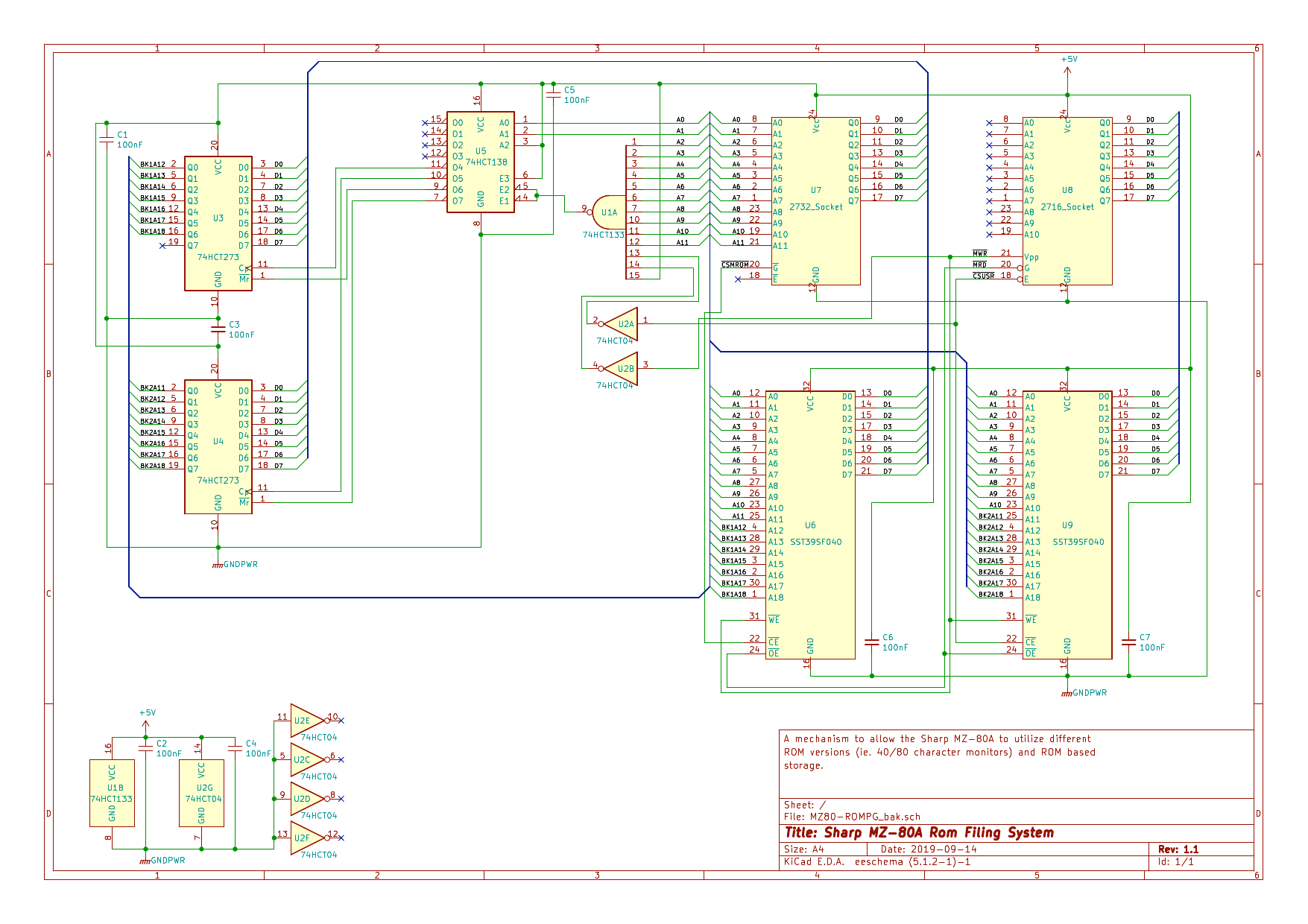
v1.1 Combined Schematic
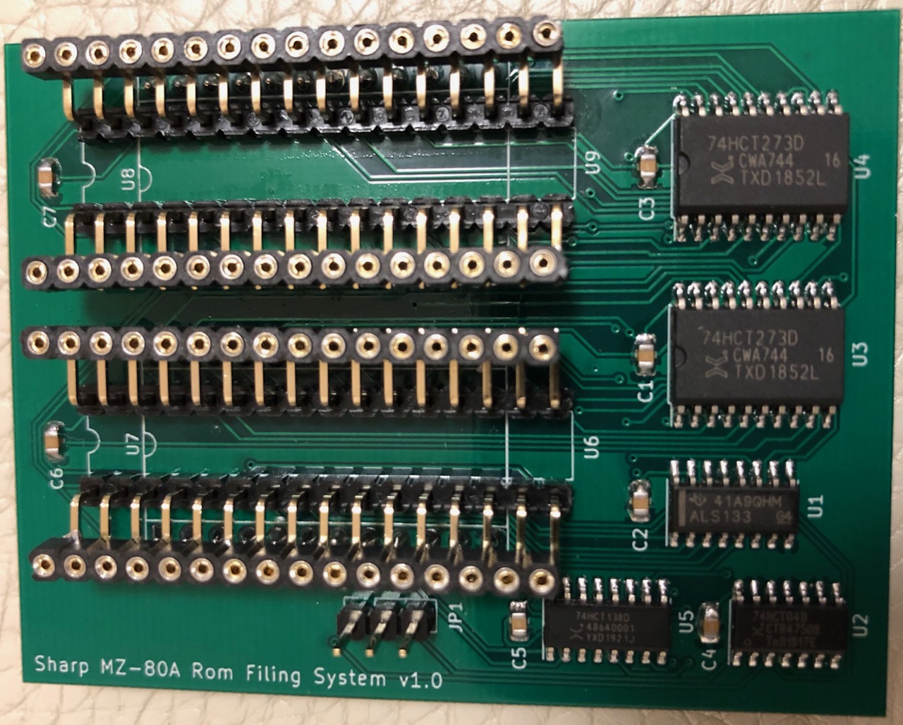
v1.1 PCB
Version 1.0 PCB (which became v1.1 with minor changes). Originally I planned to use skinny dip memory devices but changed to PDIP and had to adapt the board accordingly.
v2.0
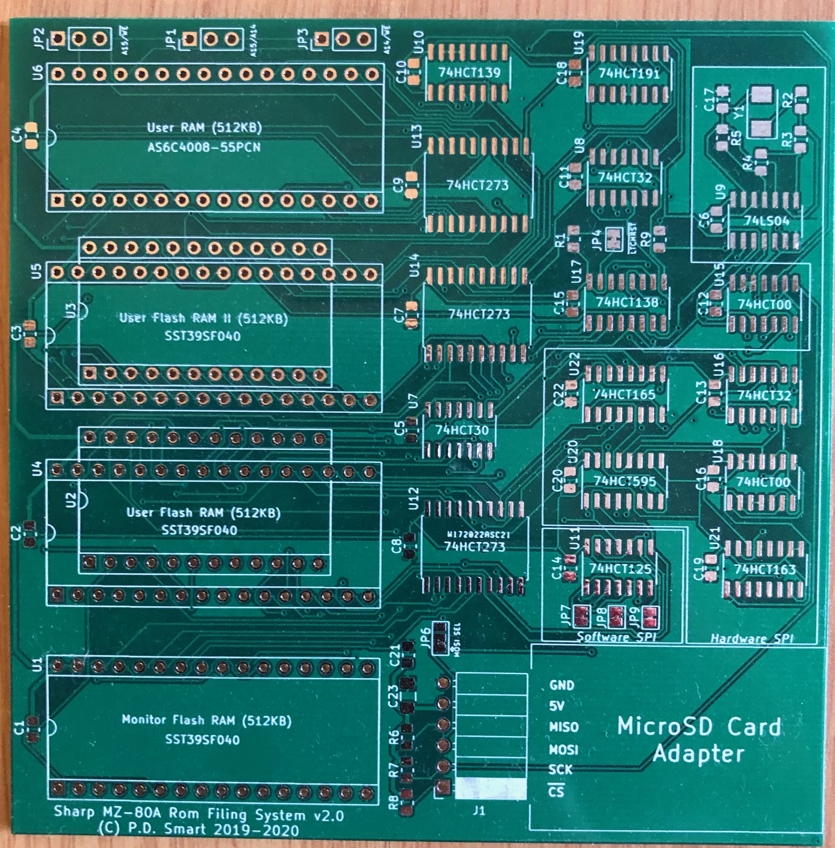
The SD card started off as a bigbang development using a Sharp Parallel printer card, which enabled the software and basic framework to be developed. The design then went further by adding a hardware SPI circuit. The hardware circuit is almost as quick as the Flash RAM devices whereas the software SPI circuit is faster than a floppy disk but noticeably slower than ROM.
Having ported CP/M (by writing a custom CBIOS) to run under the Rom Filing System on the Rom Disk, I noticed the shortfalls in lack of RAM, where even with ROM banking I could only make 46K available to CP/M and programs such as the venerable Star Trek V2 failed to run. In order to address this issue an additional 512K RAM device was added which could be paged in 2K segments. This RAM would make available storage space for CP/M structures such as control blocks and variables in order to free up more space.
All the above came together as the v2.0 design and the schematics/pcb details are in the sub-section below.
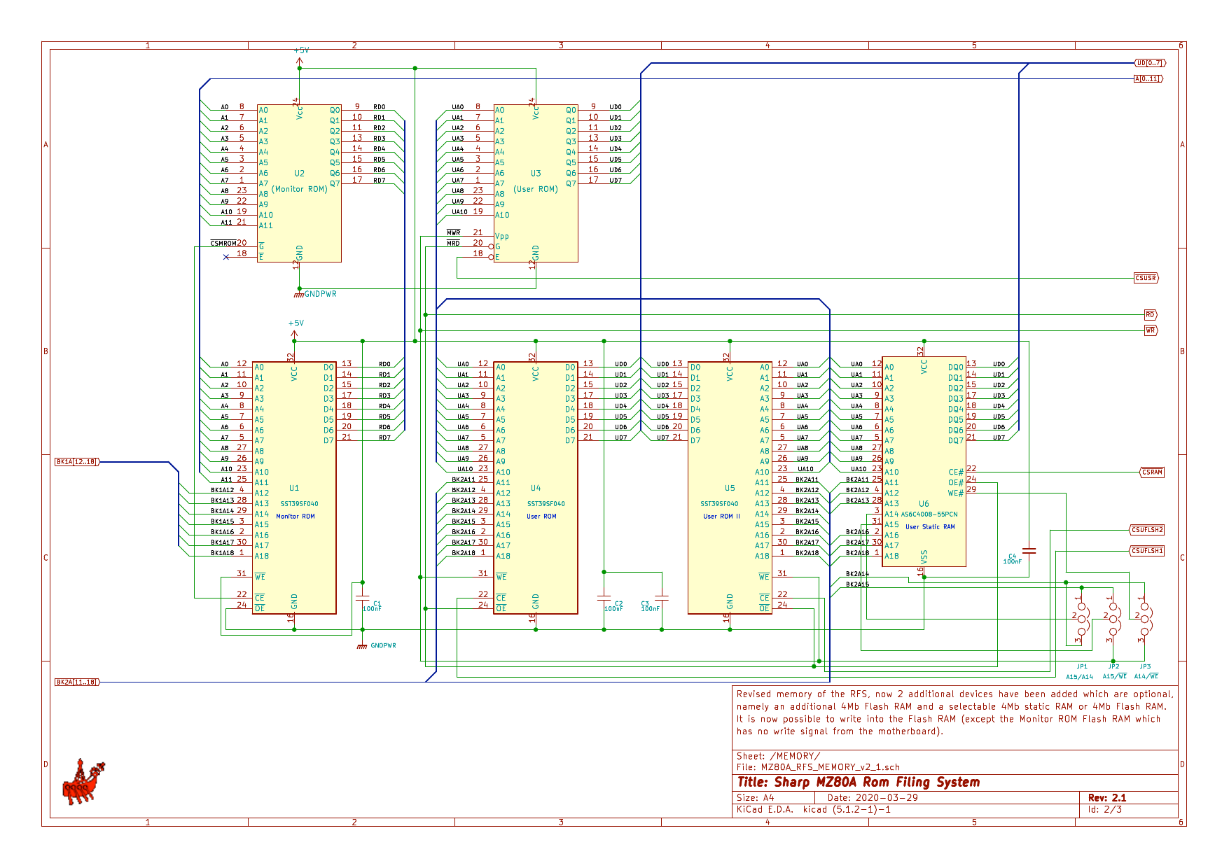
v2.0 Memory Schematic
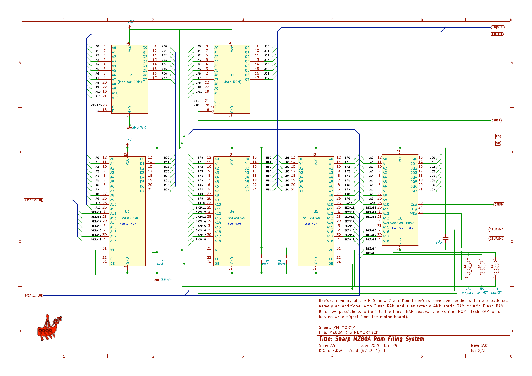
The schematic has been split into two distinct functions, Memory and Control logic. Above is the new Memory schematic which retains the single 512K Flash RAM which replaces the Monitor ROM, write access is not possible as the underlying Sharp hardware blocks write on Monitor ROM select. In the User ROM socket are 3 devices, the 512K Flash RAM from version 1 but with write access and an additional 2 devices.
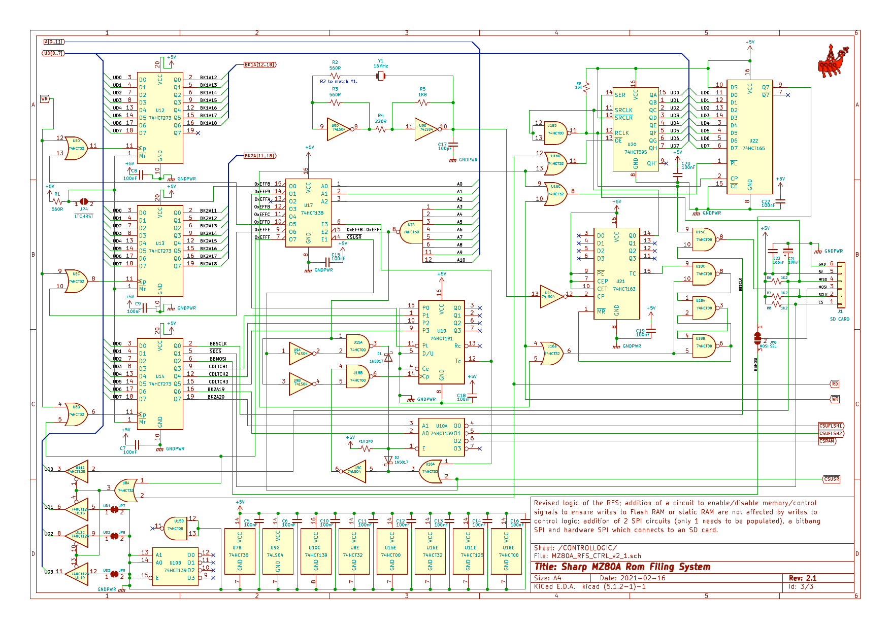
v2.0 Control Logic Schematic
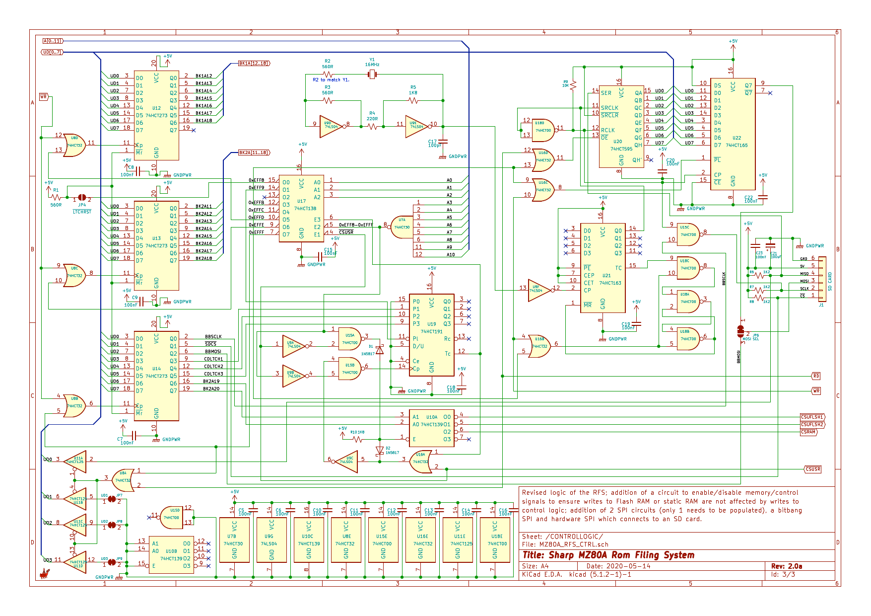
A coded latch is added (74HCT191) which only enables I/O when a read is made to the region 0xEFF8-0xEFFF for a programmable number of times. The latch U14 bits 5:3 control the number of read operations needed to active the 74HCT191. At start up U14 bits 5:3 will be 0 and to enable I/O you need to perform 16 read operations in the region 0xEFF8-0xEFFF to activate the 74HCT191 TC (terminal count) which in turn will enable the I/O control registers in the region, ie. 0xEFF8-0xEFFF. When the control registers are active the memory region 0xE800-0xEFF7 still accesses the selected Flash RAM/RAM device. A read from the location 0xEFF9 will reset the 74HCT191 and the control registers will be deactivated, the region 0xEFF8-0xEFFF now access the selected Flash RAM/RAM.
In addition it adds 2 SPI circuits, only one of which will be assembled on the PCB according to choice. The first is a software bitbang SPI using the Z80 to form the correct serial and clock signals in order to talk to an SD Card. This method uses few hardware components but is much slower. The second is a hardware SPI running at 8MHz which is capable of transferring/receiving a byte in less time that the Z80 takes to perform a read, this allows for performance similar to the Flash RAM storage.
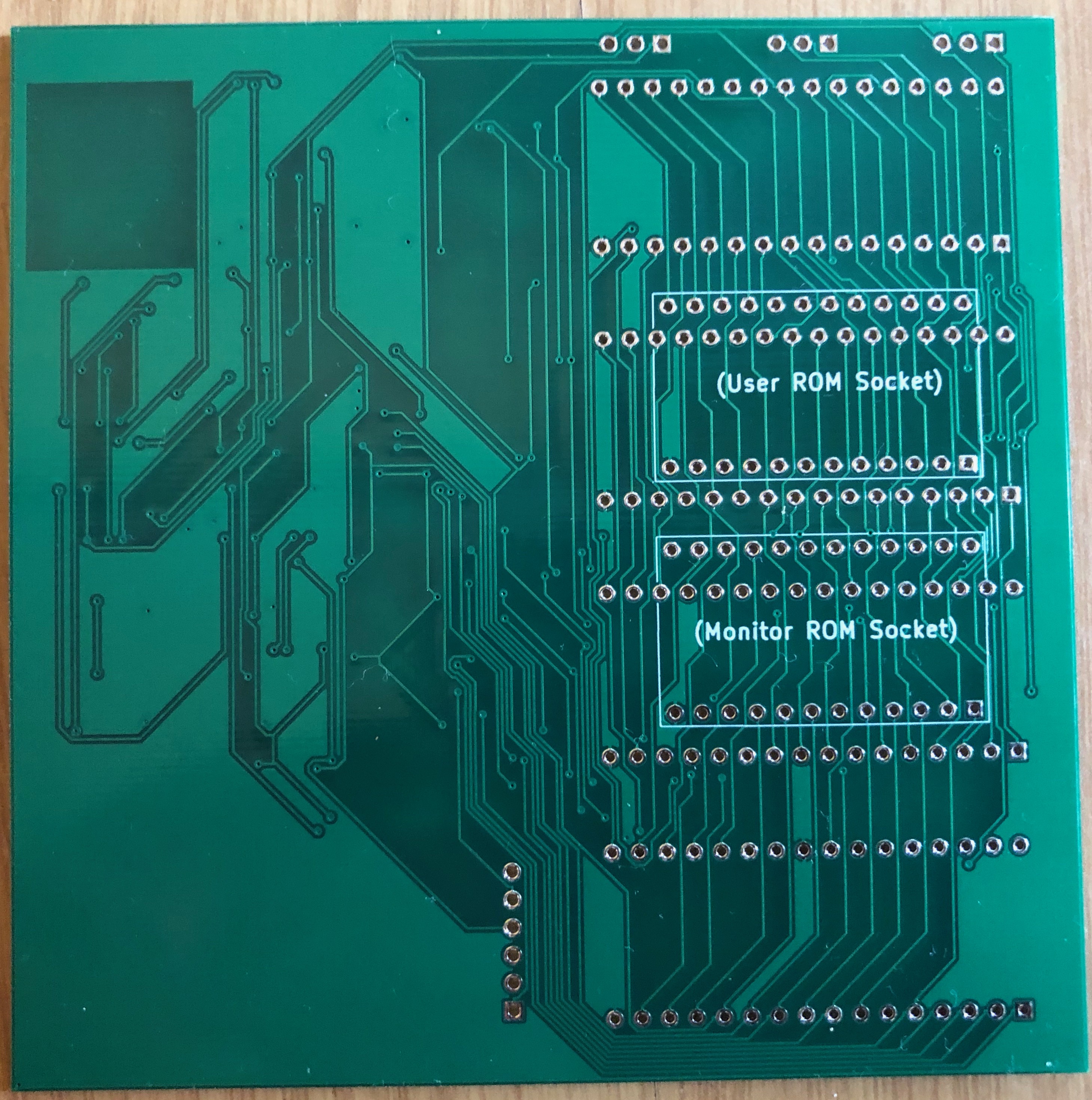
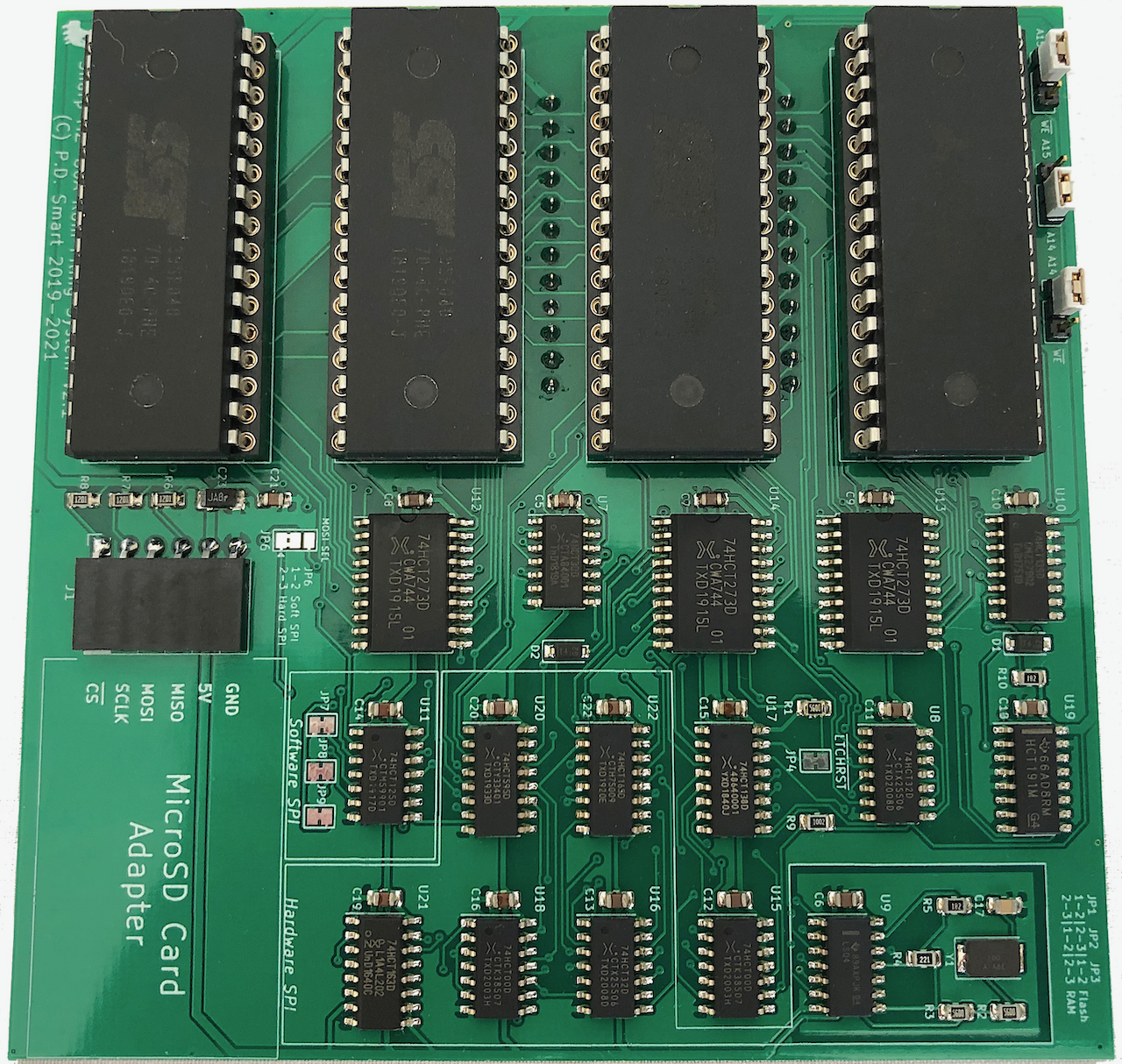
v2.0 PCB
As per previous schematics and PCB boards, this project has been designed with KiCad Schematic Capture and PCB Layout. Below are the finished boards awaiting components and assembly.
v2.1
The chance was also taken to tidy up the PCB silk screen to orient the markings as per the Sharp MZ motherboard and can be seen in the sub-section below.
v2.1 Memory Schematic
Nothing has changed on the memory schematic between the original v2.0 and v2.1 designs.
v2.1 Control Logic Schematic
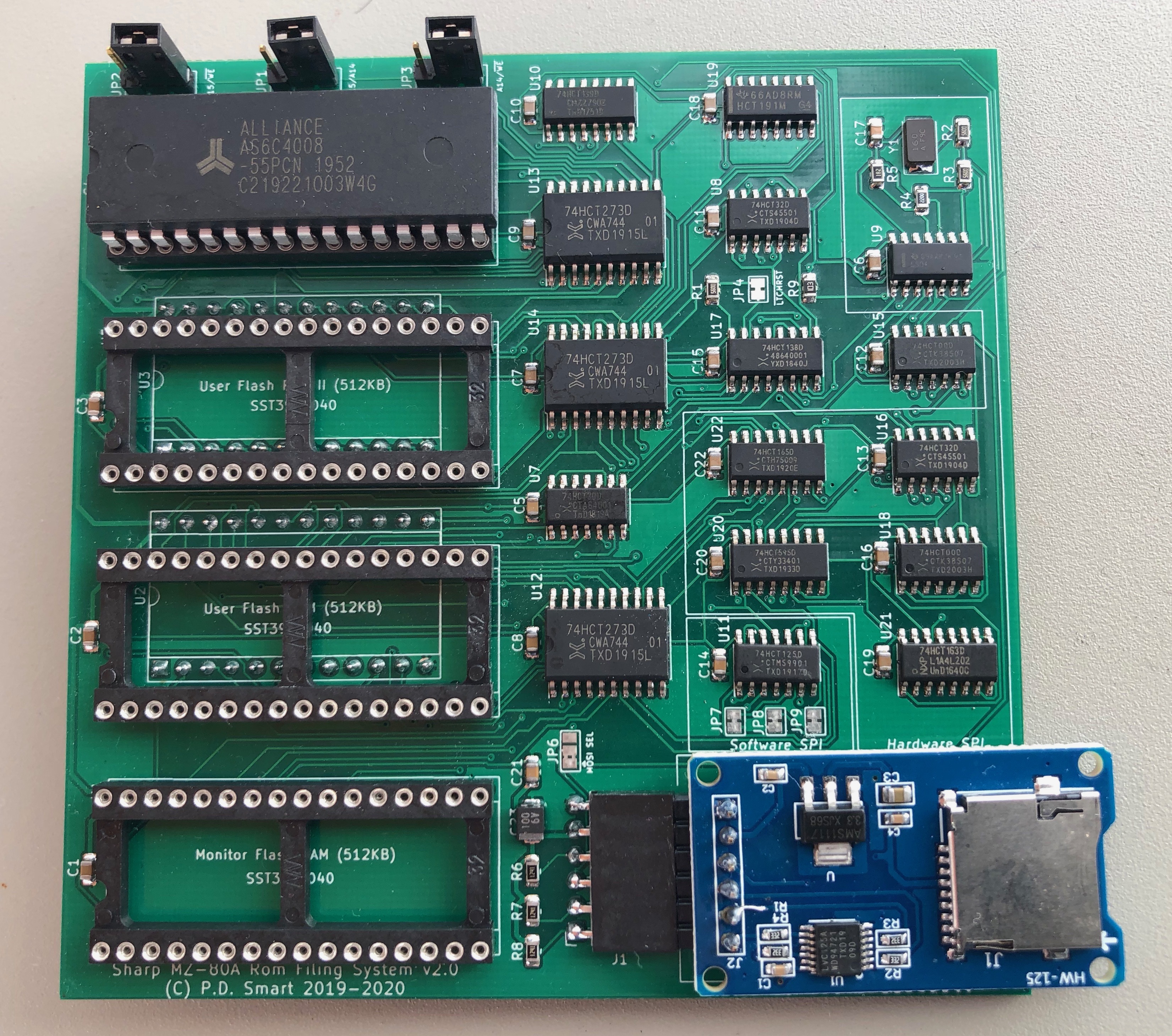
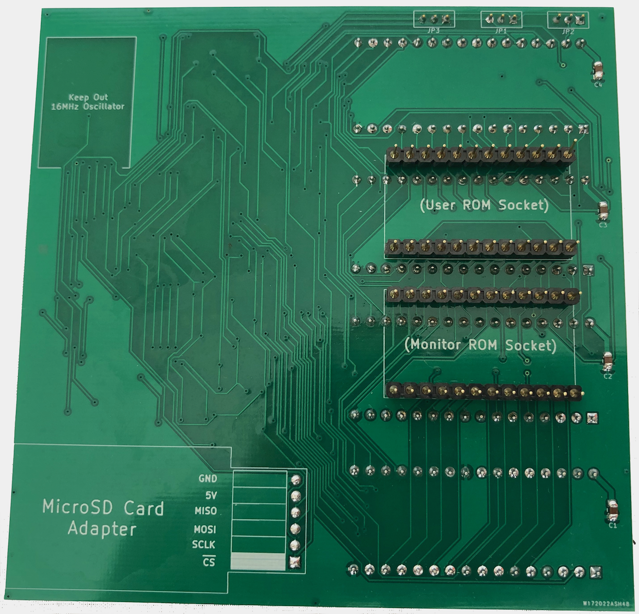
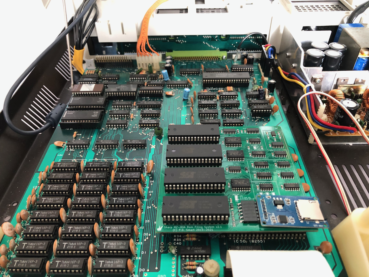
v2.1 PCB
As per previous schematics and PCB boards, this project has been designed with KiCad Schematic Capture and PCB Layout. Below are the assembled PCB's along with installation in an MZ-80A.
Rom Disk Software
Rom Filing System
One of the Flash RAM's is paged into the Monitor ROM socket and the other Flash RAM/Static RAM into the User ROM socket. The first 32Kbytes (8 slots x 4K) of the Monitor Flash RAM and the first 24Kybtes (12 slots of 2K) of the User Flash RAM is dedicated to paged ROMs with the remainder being used to store Sharp MZF format binary images compacted within 256byte sectors and additional 2K paged Static RAM.
Please refer to the Rom Filing System document for further details on the software.
(NB. The sector size may change to 128 byte sectors as the original reason for choosing 256 byte sectors no longer exists).
Sharp MZ-700 Mode
In order to cater for this upgrade, RFS has been updated to include the MZ-700 1Z-013A monitor ROM and a command to enable it. When enabled, the machine is set to compatibility mode, the 1Z-013A ROM loaded as the primary monitor and reset. The keyboard is remapped real time and so is the memory. Loading S-BASIC, read/write cassette etc works as expected on an MZ-700 whilst phyically running in an MZ-80A.
Obtaining a Rom Disk
An MZ-80A Rom Disk can be sourced on Tindie fully built or as a kit of parts (with the Flash ROMS pre-programmed). Alternatively, use the bill of materials below to purchase the parts from your local suppliers/Ebay.
Required Skill Level
Assembly of the PCB requires good SMD soldering skills and a proven technique is as follows:
- Using a nano-solder paste in a syringe, inject a little solder onto each pad.
- Place components onto the pads, smudging or bridges are not so critical (so long as you dont place excessive solder onto the pad) as the solder consolidates around the source of heat so bridges dont tend to be an issue.
- Using a 0.5mm solder bit at approx 350’c, touch each IC and component pin. If a bridge does form, use a needle, whilst applying heat, to draw out the bridge.
- Alternatively, use a heat gun at 350’c with fine nozzle and low fan speed, heat up a small section of components until the solder flows and bonds.
- On completion, wash the assembled board in Isopropyl Alcohol to remove any surplus nano-solder or flux.
Variations on the above can be made using an IR oven (or even a kitchen oven if it reaches 350’c), placing the board complete with solder and components into the oven, watching and waiting until the solder melts then remove and cool. You may need to make some slight corrections to any part which has bridged or not bonded well.
Bill Of Materials
The cost to make a Rom Disk v2.1 can be seen in the table below. This excludes consumables such as solder paste and flux. Please scroll right to see the full table details.
Source: MZ80-ROMPG_v2_1.sch
Component Count: 68
| Ref | Qty | Price (Unit) | Price (10) | Price (100) | Price Ea (5 Off Sum) | Price Ea (10 Off) | Value | Cmp name | Footprint | Description | Vendor | ||
|---|---|---|---|---|---|---|---|---|---|---|---|---|---|
| C2, C1, C3, C4, C6, C5, C12, C8, C9, C7, C15, C18, C10, C22, C20, C19, C11, C21, C13, C14, C16, | 21 | 0.2232 | 0.2232 | 0.1117 | 4.6872 | 2.3457 | 100nF | C_Small | Capacitor_SMD:C_0805_2012Metric_Pad1.15x1.40mm_HandSolder | Unpolarized capacitor, small symbol | https://uk.farnell.com/multicomp/mc0805f104m500ct/cap-0-1-f-50v-20-y5v-0805/dp/2627484 | ||
| C17, | 1 | 0.0641 | 0.0641 | 0.0641 | 0.0641 | 100pF | C_Small | Capacitor_SMD:C_0805_2012Metric_Pad1.15x1.40mm_HandSolder | Unpolarized capacitor, small symbol | https://uk.farnell.com/vishay/tmcma0j107mtrf/cap-100-f-6-3v-20/dp/2491474 | |||
| C23, | 1 | 0.7116 | 0.7116 | 0.7116 | 0.7116 | 100uF | CP_Small | Capacitor_SMD:C_1206_3216Metric_Pad1.42x1.75mm_HandSolder | Polarized capacitor, small symbol | https://uk.farnell.com/kemet/c0805c101j1gactu/cap-100pf-100v-5-c0g-np0-0805/dp/1414655 | |||
| D2, D1, | 2 | 0.358 | 0.213 | 0.716 | 0.426 | 1N5817 | 1N5817 | Diode_SMD:D_SOD-123 | 20V 1A Schottky Barrier Rectifier Diode, DO-41 | https://www.mouser.co.uk/ProductDetail/821-B0520LWRHG | |||
| J1, | 1 | 0.582 | 0.582 | 0.582 | 0.582 | SD CARD | Conn_01x06 | Connector_PinSocket_2.54mm:PinSocket_1x06_P2.54mm_Horizontal | Generic connector, single row, 01x06, script generated (kicad-library-utils/schlib/autogen/connector/) | https://uk.farnell.com/wurth-elektronik/613006143121/connector-rcpt-6pos-1row-2-54mm/dp/2827951 | |||
| JP1, | 1 | 0.2652 | 0.22 | 0.2652 | 0.22 | A15/A14 | Jumper_NC_Dual | Connector_PinHeader_2.00mm:PinHeader_1x03_P2.00mm_Vertical | Dual jumper, normally closed | https://uk.farnell.com/te-connectivity/2355045-3/connector-header-3pos-1row-2mm/dp/3289742 | |||
| JP2, | 1 | 0.2652 | 0.22 | 0.2652 | 0.22 | A15/~WE~ | Jumper_NC_Dual | Connector_PinHeader_2.00mm:PinHeader_1x03_P2.00mm_Vertical | Dual jumper, normally closed | https://uk.farnell.com/te-connectivity/2355045-3/connector-header-3pos-1row-2mm/dp/3289742 | |||
| JP3, | 1 | 0.2652 | 0.22 | 0.2652 | 0.22 | A14/~WE~ | Jumper_NC_Dual | Connector_PinHeader_2.00mm:PinHeader_1x03_P2.00mm_Vertical | Dual jumper, normally closed | https://uk.farnell.com/te-connectivity/2355045-3/connector-header-3pos-1row-2mm/dp/3289742 | |||
| Jumper, JP1-3 | 3 | 0.057 | 0.057 | 0.171 | 0.171 | 2 pin jumper | https://uk.farnell.com/multicomp/mc-2205bg/mini-shunt-jumper-2way-2mm-pbt/dp/2834677 | ||||||
| JP4, | 1 | 0 | 0 | 0 | 0 | ~LTCHRST~ | SolderJumper_2_Open | Jumper:SolderJumper-2_P1.3mm_Bridged_Pad1.0x1.5mm | Solder Jumper, 2-pole, open | ||||
| JP6, | 1 | 0 | 0 | 0 | 0 | MOSI SEL | SolderJumper_3_Bridged12 | Jumper:SolderJumper-3_P1.3mm_Bridged2Bar12_Pad1.0x1.5mm | 3-pole Solder Jumper, pins 1+2 closed/bridged | ||||
| JP7, | 1 | 0 | 0 | 0 | 0 | UD1 | SolderJumper_2_Bridged | Jumper:SolderJumper-2_P1.3mm_Bridged_Pad1.0x1.5mm | Solder Jumper, 2-pole, closed/bridged | ||||
| JP8, | 1 | 0 | 0 | 0 | 0 | UD2 | SolderJumper_2_Bridged | Jumper:SolderJumper-2_P1.3mm_Bridged_Pad1.0x1.5mm | Solder Jumper, 2-pole, closed/bridged | ||||
| JP9, | 1 | 0 | 0 | 0 | 0 | UD3 | SolderJumper_2_Bridged | Jumper:SolderJumper-2_P1.3mm_Bridged_Pad1.0x1.5mm | Solder Jumper, 2-pole, closed/bridged | ||||
| LG1, | 1 | 0 | 0 | 0 | 0 | Argo Logo | MountingHole | Graphic:Argo | Mounting Hole without connection | ||||
| R3, R2, R1, | 3 | 0.122 | 0.045 | 0.366 | 0.135 | 560R | R_Small_US | Resistor_SMD:R_0805_2012Metric_Pad1.15x1.40mm_HandSolder | Resistor, small US symbol | https://www.mouser.co.uk/ProductDetail/71-CRCW0805560RFKEAC | |||
| R4, | 1 | 0.0106 | 0.0106 | 0.0106 | 0.0106 | 220R | R_Small_US | Resistor_SMD:R_0805_2012Metric_Pad1.15x1.40mm_HandSolder | Resistor, small US symbol | https://uk.farnell.com/walsin/wr08x2200ftl/res-220r-1-150v-0805-thick-film/dp/2502698 | |||
| R5, R10, | 2 | 0.077 | 0.017 | 0.154 | 0.034 | 1K8 | R_Small_US | Resistor_SMD:R_0805_2012Metric_Pad1.15x1.40mm_HandSolder | Resistor, small US symbol | https://www.mouser.co.uk/ProductDetail/652-CR0805JW-182ELF | |||
| R8, R7, R6, | 3 | 0.077 | 0.018 | 0.231 | 0.054 | 1K2 | R_Small_US | Resistor_SMD:R_0805_2012Metric_Pad1.15x1.40mm_HandSolder | Resistor, small US symbol | https://www.mouser.co.uk/ProductDetail/652-CR0805FX-1151ELF | |||
| R9, | 1 | 0.077 | 0.045 | 0.077 | 0.045 | 10K | R_Small_US | Resistor_SMD:R_0805_2012Metric_Pad1.15x1.40mm_HandSolder | Resistor, small US symbol | https://www.mouser.co.uk/ProductDetail/71-CRCW080510K0FKEAC | |||
| U2, | 2 | 2.22 | 1.87 | 4.44 | 3.74 | (Monitor ROM) | 2732_Socket | Package_DIP:DIP-24_W15.24mm_Socket | REPROM 4 Ko | https://uk.rs-online.com/web/p/pcb-sockets/1981590/?relevancy-data=7365617263685F636173636164655F6F726465723D31267365617263685F696E746572666163655F6E616D653D4931384E53656172636847656E65726963267365617263685F6C616E67756167655F757365643D656E267365617263685F6D617463685F6D6F64653D6D61746368616C6C7061727469616C267365617263685F7061747465726E5F6D6174636865643D5E5B5C707B4C7D5C707B4E647D2D2C2F255C2E5D2B24267365617263685F7061747465726E5F6F726465723D313333267365617263685F73745F6E6F726D616C697365643D59267365617263685F726573706F6E73655F616374696F6E3D267365617263685F747970653D4B4559574F52445F53494E474C455F414C5048415F4E554D45524943267365617263685F7370656C6C5F636F72726563745F6170706C6965643D59267365617263685F77696C645F63617264696E675F6D6F64653D4E4F4E45267365617263685F6B6579776F72643D5353512D3131322D30332D472D53267365617263685F6B6579776F72645F6170703D5353512D3131322D30332D472D53267365617263685F636F6E6669673D3026&searchHistory=%7B%22enabled%22%3Atrue%7D | |||
| U3, | 2 | 2.22 | 1.87 | 4.44 | 3.74 | (User ROM) | 2716_Socket | Package_DIP:DIP-24_W15.24mm_Socket | REPROM 2KO | https://uk.rs-online.com/web/p/pcb-sockets/1981590/?relevancy-data=7365617263685F636173636164655F6F726465723D31267365617263685F696E746572666163655F6E616D653D4931384E53656172636847656E65726963267365617263685F6C616E67756167655F757365643D656E267365617263685F6D617463685F6D6F64653D6D61746368616C6C7061727469616C267365617263685F7061747465726E5F6D6174636865643D5E5B5C707B4C7D5C707B4E647D2D2C2F255C2E5D2B24267365617263685F7061747465726E5F6F726465723D313333267365617263685F73745F6E6F726D616C697365643D59267365617263685F726573706F6E73655F616374696F6E3D267365617263685F747970653D4B4559574F52445F53494E474C455F414C5048415F4E554D45524943267365617263685F7370656C6C5F636F72726563745F6170706C6965643D59267365617263685F77696C645F63617264696E675F6D6F64653D4E4F4E45267365617263685F6B6579776F72643D5353512D3131322D30332D472D53267365617263685F6B6579776F72645F6170703D5353512D3131322D30332D472D53267365617263685F636F6E6669673D3026&searchHistory=%7B%22enabled%22%3Atrue%7D | |||
| U2/U3 Straight Pin Header | 4 | 1.504 | 1.504 | 6.016 | 6.016 | https://uk.rs-online.com/web/p/pcb-headers/6742309/?relevancy-data=7365617263685F636173636164655F6F726465723D31267365617263685F696E746572666163655F6E616D653D4931384E525353746F636B4E756D626572267365617263685F6C616E67756167655F757365643D656E267365617263685F6D617463685F6D6F64653D6D61746368616C6C267365617263685F7061747465726E5F6D6174636865643D5E2828282872737C5253295B205D3F293F285C647B337D5B5C2D5C735D3F5C647B332C347D5B705061415D3F29297C283235285C647B387D7C5C647B317D5C2D5C647B377D29292924267365617263685F7061747465726E5F6F726465723D31267365617263685F73745F6E6F726D616C697365643D59267365617263685F726573706F6E73655F616374696F6E3D267365617263685F747970653D52535F53544F434B5F4E554D424552267365617263685F77696C645F63617264696E675F6D6F64653D4E4F4E45267365617263685F6B6579776F72643D3637342D32333039267365617263685F6B6579776F72645F6170703D36373432333039267365617263685F636F6E6669673D3026&searchHistory=%7B%22enabled%22%3Atrue%7D | |||||||
| U1,U4,U5,U6 32pin Turned Pin Socket | 4 | 0.774 | 0.774 | 3.096 | 3.096 | https://uk.rs-online.com/web/p/dil-sockets/1974081/?relevancy-data=7365617263685F636173636164655F6F726465723D31267365617263685F696E746572666163655F6E616D653D4931384E525353746F636B4E756D626572267365617263685F6C616E67756167655F757365643D656E267365617263685F6D617463685F6D6F64653D6D61746368616C6C267365617263685F7061747465726E5F6D6174636865643D5E2828282872737C5253295B205D3F293F285C647B337D5B5C2D5C735D3F5C647B332C347D5B705061415D3F29297C283235285C647B387D7C5C647B317D5C2D5C647B377D29292924267365617263685F7061747465726E5F6F726465723D31267365617263685F73745F6E6F726D616C697365643D59267365617263685F726573706F6E73655F616374696F6E3D267365617263685F747970653D52535F53544F434B5F4E554D424552267365617263685F77696C645F63617264696E675F6D6F64653D4E4F4E45267365617263685F6B6579776F72643D3139372D34303831267365617263685F6B6579776F72645F6170703D31393734303831267365617263685F636F6E6669673D3026&searchHistory=%7B%22enabled%22%3Atrue%7D | |||||||
| U5, U4, U1, | 2 | 1.4 | 1.34 | 2.8 | 2.68 | SST39SF040 | SST39SF040-Memory_Flash | Package_DIP:DIP-32_W15.24mm_Socket | https://www.mouser.co.uk/ProductDetail/804-39SF0407CPHE | ||||
| U6, | 1 | 4.04 | 3.52 | 4.04 | 3.52 | AS6C4008-55PCN | AS6C4008-55PCN-Memory_RAM | Package_DIP:DIP-32_W15.24mm_Socket | https://uk.rs-online.com/web/p/sram/7444561/?cm_mmc=UK-PPC-DS3A-_-google-_-DSA_UK_EN_Semiconductors_Index-_-SRAM%7C+Products-_-DYNAMIC+SEARCH+ADS&matchtype=b&aud-826607888587:dsa-1212641595354&s_kwcid=AL!7457!3!504893415565!b!!g!!&gclid=Cj0KCQjw4cOEBhDMARIsAA3XDRh4TCTF_wYFuxNMcgRPi_SnsWjU6rH-V_O0fBiKy5KjJ19J3uHoBHIaAuSTEALw_wcB&gclsrc=aw.ds | ||||
| U7, | 1 | 0.374 | 0.286 | 0.374 | 0.286 | 74HCT30 | 74LS30 | Package_SO:SOIC-14_3.9x8.7mm_P1.27mm | 8-input NAND | https://www.mouser.co.uk/ProductDetail/771-HCT30D653 | |||
| U8, U16, | 2 | 0.343 | 0.257 | 0.686 | 0.514 | 74HCT32 | 74LS32 | Package_SO:SOIC-14_3.9x8.7mm_P1.27mm | Quad 2-input OR | https://www.mouser.co.uk/ProductDetail/771-74HCT32D-T | |||
| U9, | 1 | 0.58 | 0.479 | 0.58 | 0.479 | 74LS04 | 74LS04 | Package_SO:SOIC-14_3.9x8.7mm_P1.27mm | Hex Inverter | https://www.mouser.co.uk/ProductDetail/595-SN74LS04DR | |||
| U10, | 1 | 0.328 | 0.274 | 0.328 | 0.274 | 74HCT139 | 74LS139 | Package_SO:SOIC-16_3.9x9.9mm_P1.27mm | Dual Decoder 1 of 4, Active low outputs | https://www.mouser.co.uk/ProductDetail/771-74HCT139D-Q100J | |||
| U11, | 1 | 0.252 | 0.207 | 0.252 | 0.207 | 74HCT125 | 74LS125 | Package_SO:SOIC-14_3.9x8.7mm_P1.27mm | Quad buffer 3-State outputs | https://www.mouser.co.uk/ProductDetail/771-74HCT125D-T | |||
| U12, U14, U13, | 3 | 0.374 | 0.319 | 1.122 | 0.957 | 74HCT273 | 74HCT273 | Package_SO:SOIC-20W_7.5x12.8mm_P1.27mm | 8-bit D Flip-Flop, reset | https://www.mouser.co.uk/ProductDetail/771-74HCT273D-T | |||
| U15, U18, | 2 | 0.343 | 0.257 | 0.686 | 0.514 | 74HCT00 | 74LS00 | Package_SO:SOIC-14_3.9x8.7mm_P1.27mm | quad 2-input NAND gate | https://www.mouser.co.uk/ProductDetail/771-74HCT00D-T | |||
| U17, | 1 | 0.282 | 0.232 | 0.282 | 0.232 | 74HCT138 | 74LS138 | Package_SO:SOIC-16_3.9x9.9mm_P1.27mm | Decoder 3 to 8 active low outputs | https://www.mouser.co.uk/ProductDetail/Nexperia/74HCT138D653?qs=P62ublwmbi8MKahyK7iY6g%3D%3D | |||
| U19, | 1 | 0.694 | 0.572 | 0.694 | 0.572 | 74HCT191 | 74LS191 | Package_SO:SOIC-16_3.9x9.9mm_P1.27mm | 4-bit Synchronous Up/Down binary Counter | https://www.mouser.co.uk/ProductDetail/595-CD74HCT191M | |||
| U20, | 1 | 0.343 | 0.281 | 0.343 | 0.281 | 74HCT595 | 74LS595 | Package_SO:SOIC-16_3.9x9.9mm_P1.27mm | 8-bit serial in/out Shift Register 3-State Outputs | https://www.mouser.co.uk/ProductDetail/771-74HCT595DQ100118 | |||
| U21, | 1 | 0.411 | 0.361 | 0.411 | 0.361 | 74HCT163 | 74LS163 | Package_SO:SOIC-16_3.9x9.9mm_P1.27mm | Synchronous 4-bit programmable binary Counter | https://www.mouser.co.uk/ProductDetail/771-HCT163D653 | |||
| U22, | 1 | 0.442 | 0.376 | 0.442 | 0.376 | 74HCT165 | 74LS165 | Package_SO:SOIC-16_3.9x9.9mm_P1.27mm | Shift Register 8-bit, parallel load | https://www.mouser.co.uk/ProductDetail/771-74HCT165D-T | |||
| Y1, | 1 | 0.442 | 0.418 | 0.442 | 0.418 | 16MHz | Crystal_Small | Crystal:Crystal_SMD_Abracon_ABM3-2Pin_5.0x3.2mm | Two pin crystal, small symbol | https://www.mouser.co.uk/ProductDetail/815-ABM3-16-B2-T | |||
| SD Card Adaptor | 1 | 2.77 | 2.6 | 2.77 | 2.6 | https://www.ebay.co.uk/itm/233362415633?hash=item36557be011:g:-xwAAOSwXk1dmxM7 | |||||||
| PCB - PCBWay | 1 | 3.7635 | 3.7635 | 3.7635 | 3.7635 | ||||||||
| Sub Total | 46.5736 | 39.8655 | |||||||||||
| P&P | 5 | 5 | |||||||||||
| VAT @ 20% | 10.315 | 8.9731 | |||||||||||
| Total (GBP) | 61.89 | 53.84 |
Credits
Licenses
The Gnu Public License v3
The source files are distributed in the hope that it will be useful, but WITHOUT ANY WARRANTY; without even the implied warranty of MERCHANTABILITY or FITNESS FOR A PARTICULAR PURPOSE. See the GNU General Public License for more details.
You should have received a copy of the GNU General Public License along with this program. If not, see http://www.gnu.org/licenses/.