 Sharp MZ80A Video Module
Overview
A study of the MZ80A hardware though revealed it was identical to the more costly business machine, the MZ80B. The hardware in the MZ80A had been wired differently to cripple its capabilities, presumably for marketing reasons, so by rerouting the wiring it is fairly easy to achieve an 80 column display.
The v1 upgrades, via rewiring and minor tweaks, utilize the MZ-80B circuit to achieve a switchable 40/80 column display on the MZ-80A.
Also, a study of the monitor ROM and the hardware indicates the MZ80A was intended to have a colour output board upgrade similar to the Sharp MZ700 but was never commercially sold. In fact, my original 1982 MZ-80A User Manual which I understand to be very rare contains the details of the colour circuit Sharp intended to produce.
Nibbles Lab (an excellent Sharp Museum and repository of information - be sure to use google chrome to auto-translate) spotted this and designed a circuit to upgrade the MZ80A so that it could output video to a colour monitor. Taking this base circuit with some modifications (composite video) I’ve added it into the v1 upgrades.
In order to achieve rerouting of wires between the video gate arrays and video shift register, the design required these ic’s to be lifted onto a daughter card. At this point I saw that the Character Generator ROM could be upgraded utilizing a modern Flash RAM which would allow for the storage and switching of multiple Character ROMS, ie. MZ80A, MZ700 I/II, Japanese MZ80K Rom etc. I settled on a 32KByte Flash RAM which can store 16 character generator ROM sets which can be switched via the attribute RAM (4 ROMS in 1 of 4 blocks) and the control register.
One of my aims in the projects is to merge, as close as possible, my Sharp MZ Hardware Emulator and real machines, expanding the capabilities of a real machine and providing real life feedback to improve the emulator. This was the reasoning for starting v2 of the Video Module which is based on FPGA technology, the same as used in the Emulator.
A caveat emptor to mention is that the hardware has been upgraded in version 2 but there may not be a lot of software. I havent spent a great deal of time yet getting for example MZ-80B SB-5510 BASIC running so pixel graphics could be used, it works on the emulator but the actual real machine may need more tweaks to run non-native software or exercise the added upgrades.
Video Module Version 1.0
- The kicad footprint editor, probably my mistake, switched the 2 VLSI gate array footprints around. Correcting this entailed fine soldering and rewiring to correct.
- The oscillator wasnt giving a clean signal so the addition of a 100pF ceramic cap between the U14B pin 4 and ground corrected this. This could be partly due to the above rewiring.
- The gatearray G signal was not connected between the two gatearrays even though it was connected in the circuit diagram, it appeared to be a PCB break.
- Attribute RAM / Control Latch clash, a write to the control latch updates the upper attribute RAM mirror locations.
- Physical Alignment of the gate arrays raiser pins and motherboard sockets was out of alignment causing difficulty in installation and stress on the pins.
I have just revisited version 1.0 of the design and resolved the original issues creating v1.1, detailed below.
v1.0 Colour Schematic
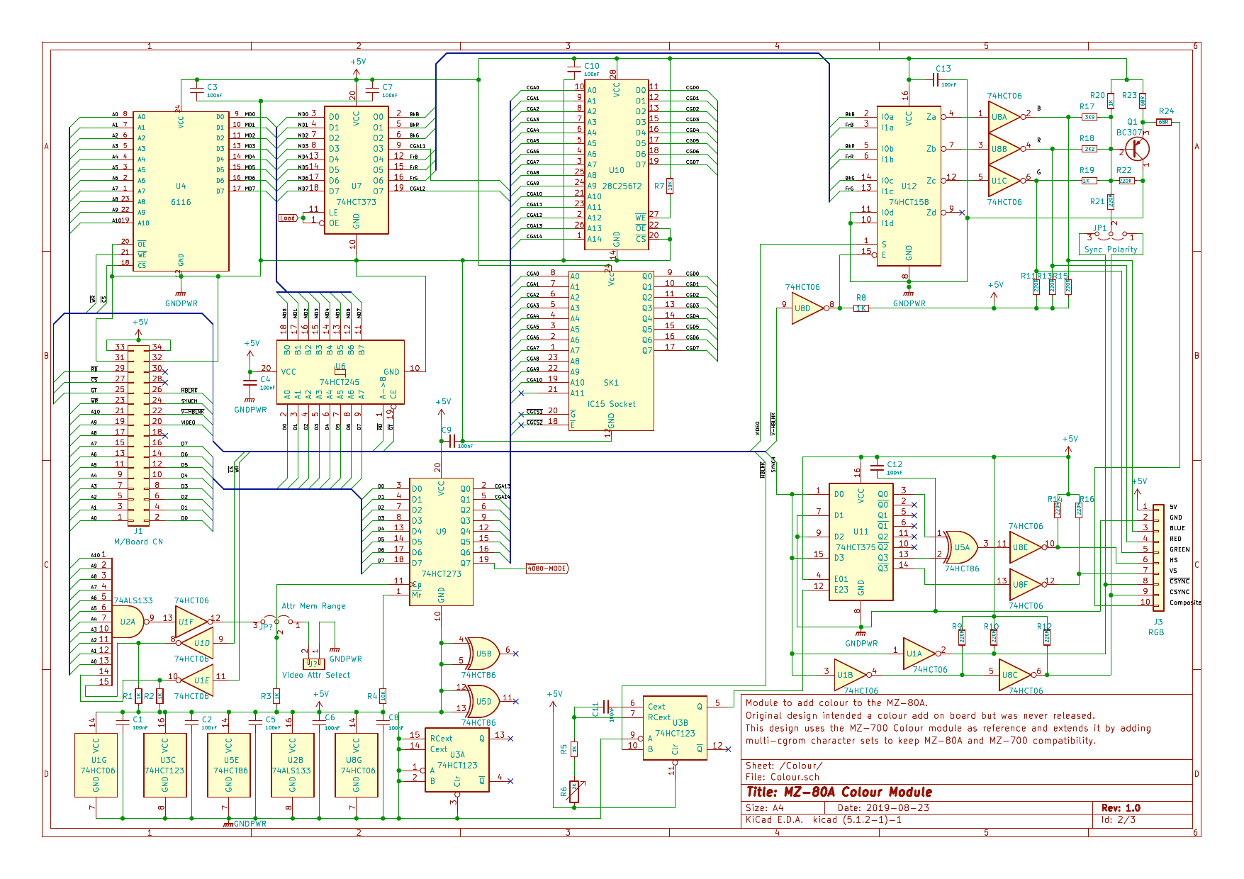
In addition to the colour generation circuit, IC15 on the motherboard, the Character Generator ROM, is lifted and replaced by IC U10, a 32KByte Flash RAM. Using bits 7 and 3 from the video attribute output stream of IC U7 and in combination with the latch IC U9, a Character Generator ROM set can be selected. The latch IC U9 selects a set of 4 out of 16 character generator sets within the 32KByte Flash RAM and the attribute bits allow subselection of the 4, thus each character can choose, via the attribute RAM, a possible 4 different character sets at any one time.
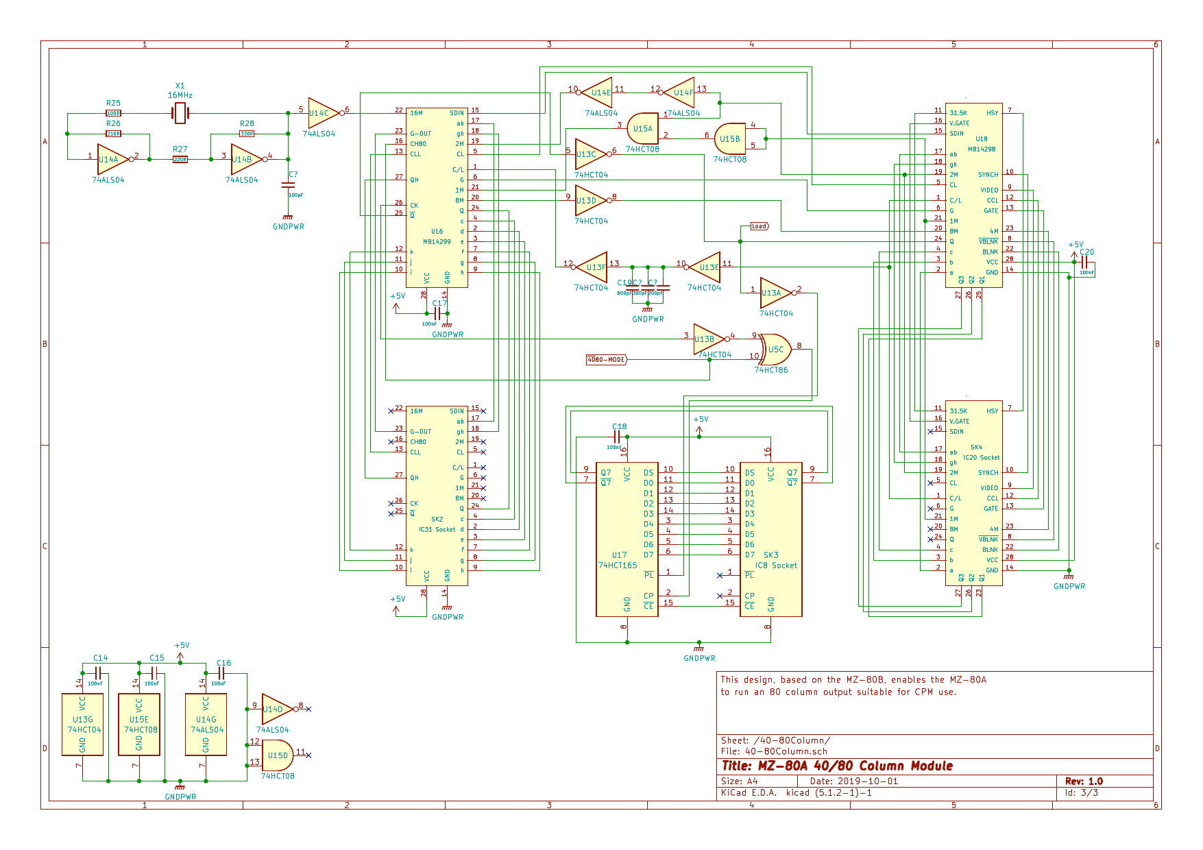
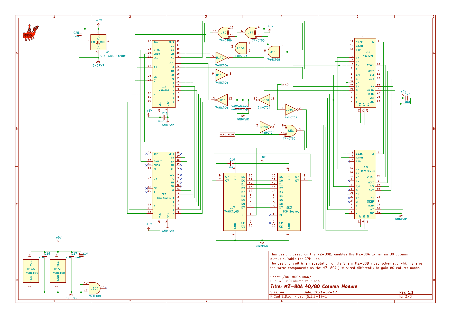
v1.0 40/80 Column Schematic
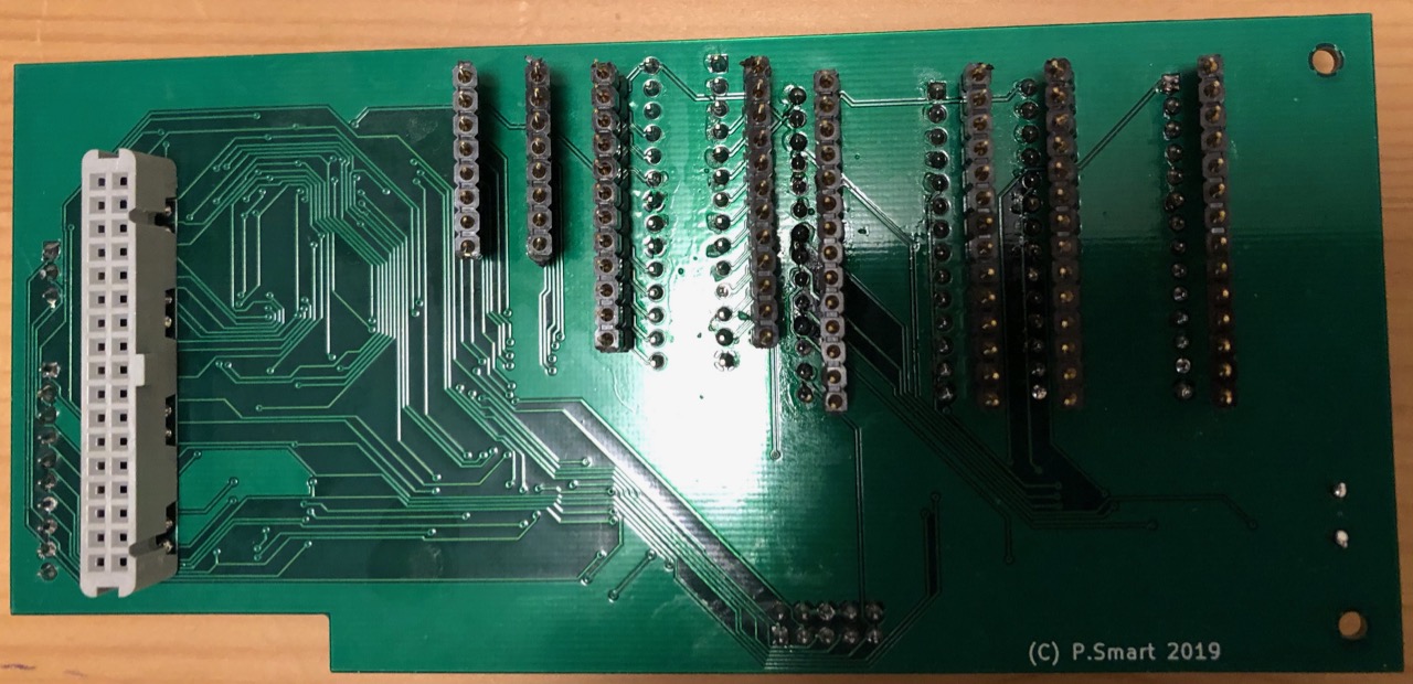
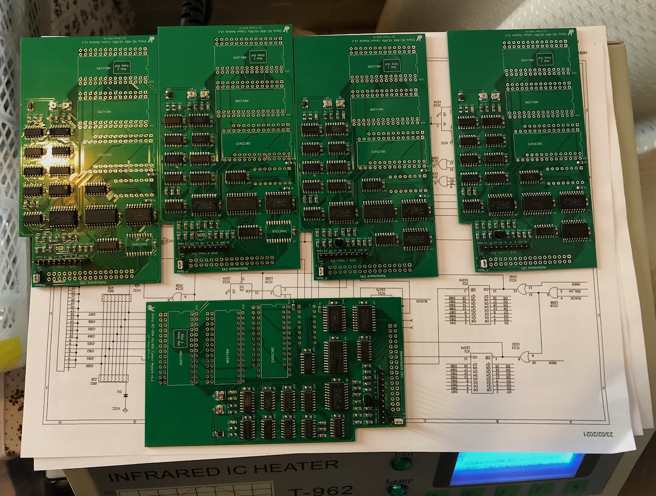
v1.0 PCB
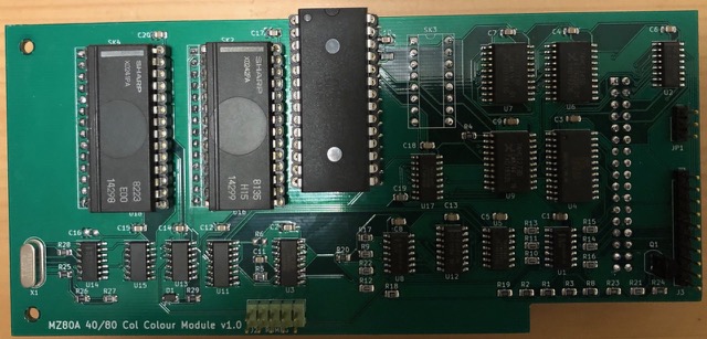
Daughter board with all the relocated IC’s in place.
Underside of the daughter board. The 34pin CN connector locates to the mainboard Video expansion connector and the remainder are standoffs to extend the original socketed IC's (removed and relocated onto the daughter card) upto the daughter board for rerouting.
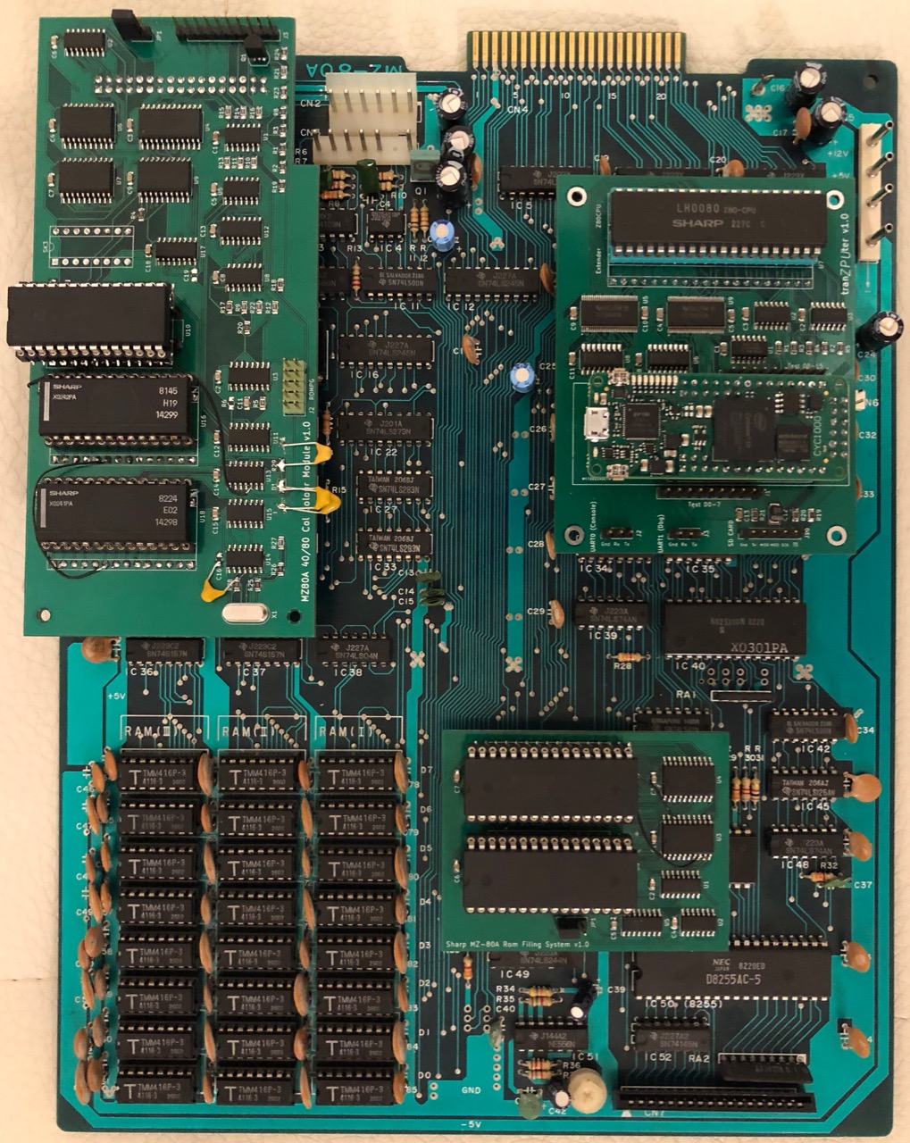
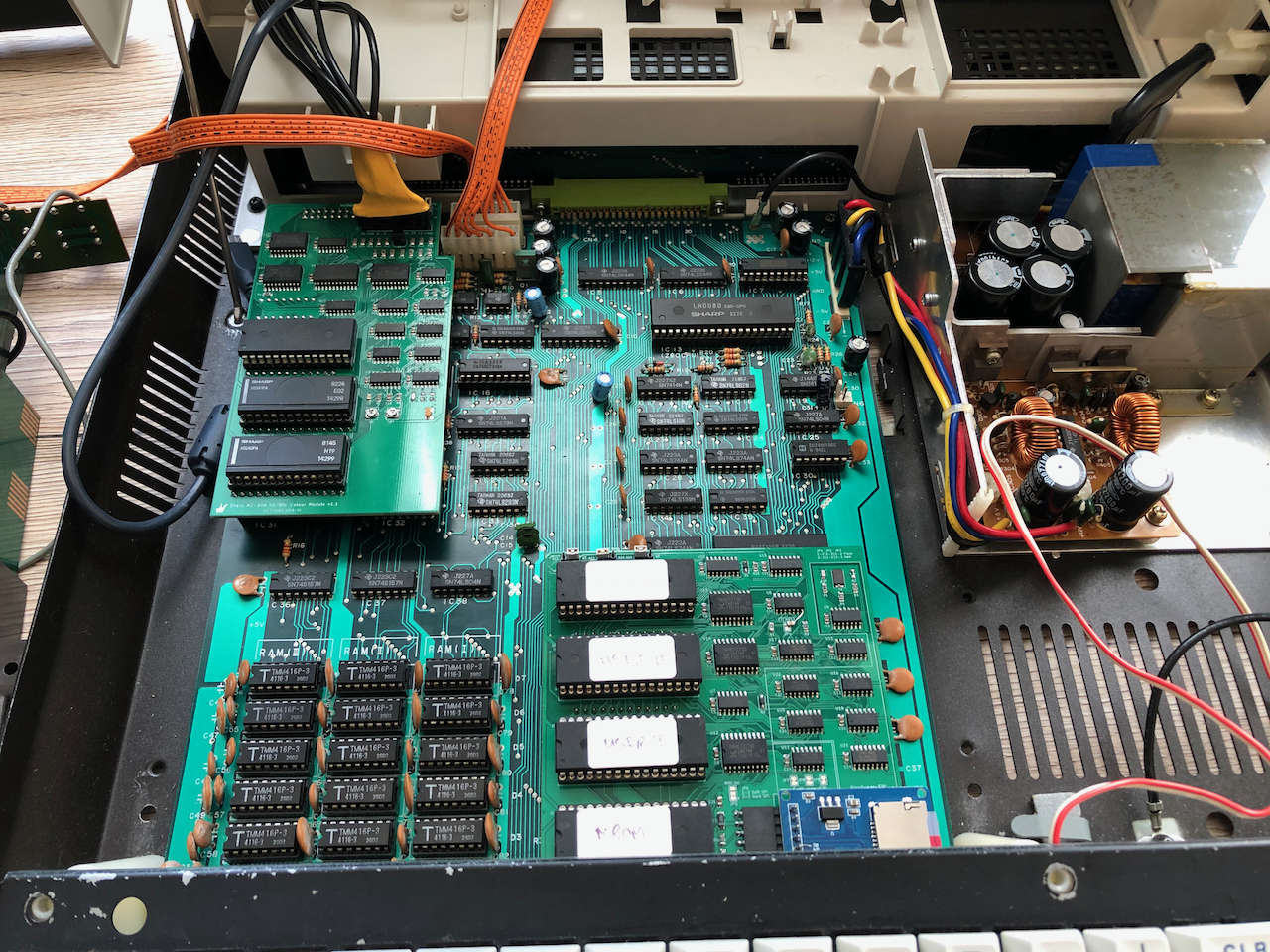
Original motherboard (above) with the daughter board in place.
Video Module Version 1.1
After an interest in the Video Module version 1 it gave me the necessary push to finish what was started and complete the task. The new design resolves the issues:
- The kicad footprint editor, probably my mistake, switched the 2 VLSI gate array footprints around. Correcting this entailed fine soldering and rewiring to correct.
- The oscillator wasnt giving a clean signal so the addition of a 100pF ceramic cap between the U14B pin 4 and ground corrected this. This could be partly due to the above rewiring.
- The gatearray G signal was not connected between the two gatearrays even though it was connected in the circuit diagram, it appeared to be a PCB break.
- Attribute RAM / Control Latch clash, a write to the control latch would update the attribute RAM. In the original design I knew this was an issue but presumed it wouldnt matter as it wouldnt be visible!
- Physical Alignment of the gate arrays raiser pins and motherboard sockets was out of alignment causing difficulty in installation and stress on the pins.
Item 4 was resolved by using the second half of the multi-vibrator (74HCT123) to elongate an enable pulse such that a read 0xDFFF followed by an immediate write 0xDFFF would go to the control latch, a read 0xDFFF followed by a NOP followed by a write 0xDFFF would go to the attribute RAM, thus ensuring read-modify-write software didnt affect the control latch.
v1.1 Colour Schematic
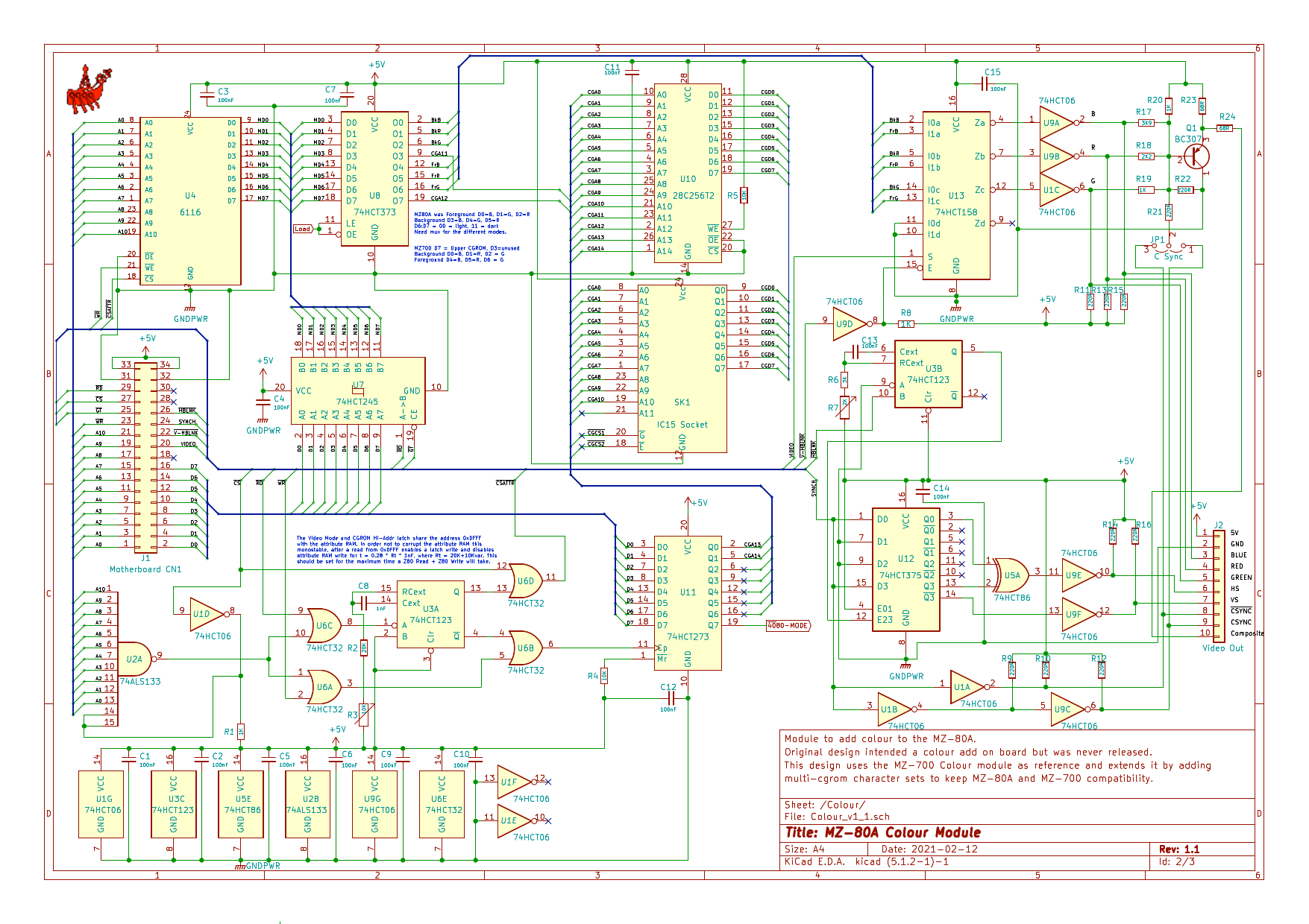
In order to allow flexibility, the resistor part has been made variable to fine tune the period between the read 0xDFFF and a subsequent write 0xDFFF.
v1.1 40/80 Column Schematic
v1.1 PCB
Version 1.1 sees the PCB being redesigned, smaller and better organised. The location of the gatearray lifter sockets was determined by using a pencil trace of the MZ-80A motherboard and using a micrometer to get accurate distances, follwed by the finished layout being printed and laid over the pencil trace to verify location. A technique I had to use on the MZ-700 as tolerances were more tight.
The PCB has been manufactured with assembly and installation as per the pictures below.
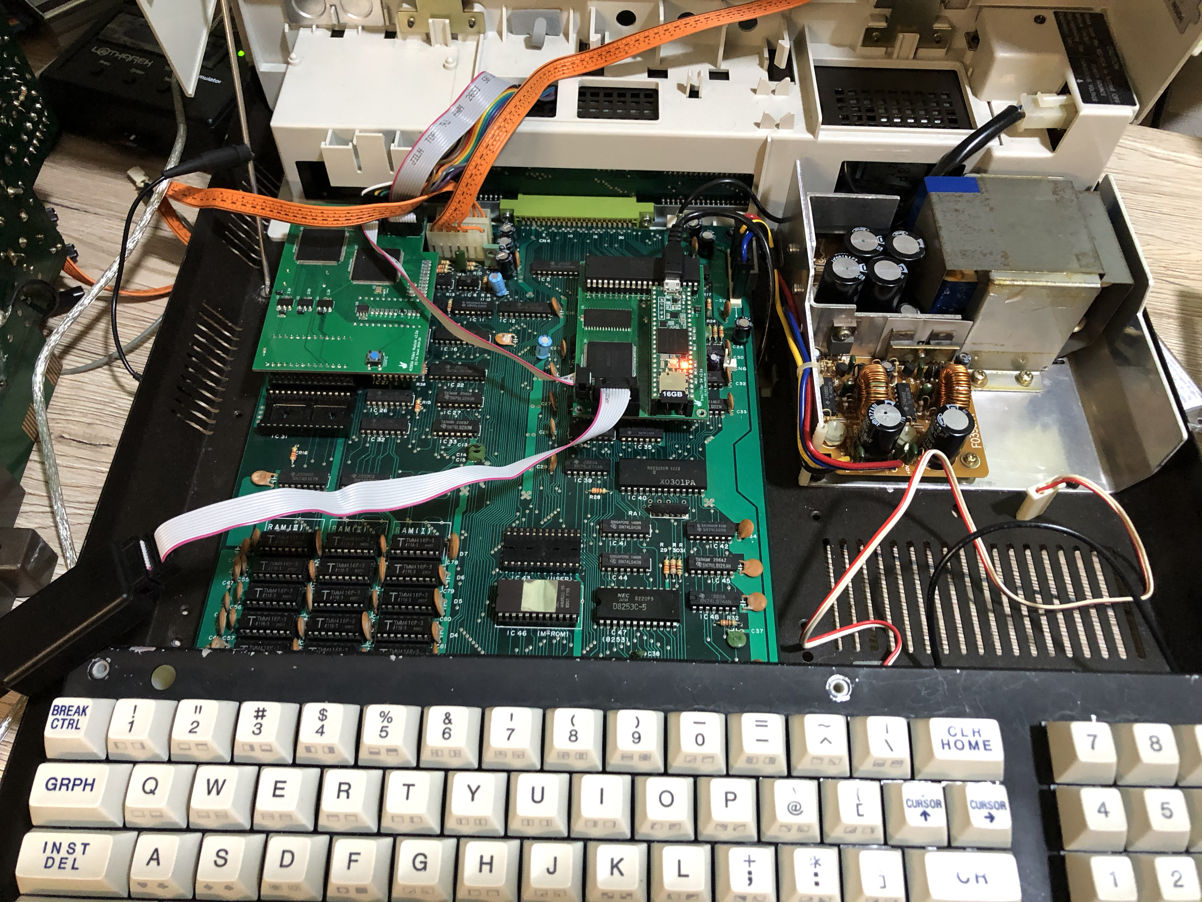
Installation inside an MZ-80A.
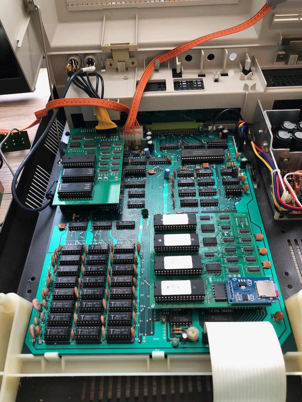
The SD Card adapter plugs in to the board but it can quite easily be relocated to a more convenient location as required. The external video connector is wired to a DIN socket which fits inside one of the body cutouts originally intended for this purpose. The second DIN socket is for USB connectivity with a tranZPUter board when installed.
v1.1 Installation Notes
In order to upgrade the video on a Sharp MZ-80A you need to be able to inject new video control signals into the serialiser IC 8 (74LS165), basically the load and clock pulse signals change according to 40/80 mode. The only way to do this is to cut tracks or remove the IC. As I dont like modifying vintage equipment I chose the later, ie. remove IC 8 and install a socket. Using this method the machine can be returned to original at any time by reinstalling the 74LS165.
If you are familiar with electronics and soldering then the modification is straight forward by following the below instructions:
1) Remove the two screws under the keyboard at the front of the machine, one in each corner.
2) Remove the 4 screws on the monitor legs.
3) Unplug the speaker cable which runs up the side of the monitor and onto a two pronged connector. NB. Dont do this if you have just switched off the monitor, wait a while.
4) At the rear of the machine just behind the CRT control signal input on the end of the CRT glass neck, to the left, is a small daughter board which holds the RESET, Volume, Brightness controls. Gently pry this loose from the two restrainers. Dont put too much pressure on the restrainers, the machine is 40 years old so they have probably lost their flexibility.
5) Trace the orange cable from the CRT to the motherboard and unplug (there are two, one is for the CRT, the other for the tape deck).
6) Just below the CRT control board, on the motherboard is a 2 pin connector with a grey wire, the RESET signal (you can trace it back from the daughter board removed in 4. Unplug it.
7) Gently lift out the CRT monitor and place in a safe location.
8) Remove the 3 screws holding the keyboard down and hinge forward.
9) At the rear of the motherboard are two screws, one in each corner, remove them.
10) Unplug the thick black earth wire coming from the PSU.
11) Unplug the PSU connector (Red, Yellow, Black and Blue wires identify it).
12) Unplug the tape deck orange cable.
13) Gently disconnect the keyboard ribbon cable, grab each side and gently pull in a rocking motion to release it from the push fit connector.
14) Gently raise and remove the motherboard, it will need a bit of back pressure. Dont try to bend the 3 plastic clips at the front of the motherboard, the plastic after 40 years is no longer as flexible as it once was!
15) Locate IC8 on the rear left side of the board, the two 28 pin Sharp branded Gate Arrays are a good locator.
16) Turn the board upside down and desolder the IC.
17) Install a 16 pin socket in the location of IC8.
18) Re-install the motherboard, again take care with the plastic clips, restore the two screws which hold it down.
19) Reconnect the black ground wire from the PSU.
20) Reconnect the PSU cable, the Red lead goes to the rear of the machine, blue faces to the front of the machine,
21) Reconnect the tape deck cable, it goes into the front most of the two similar connectors. The cable has one pin missing, that side of the connector should face to the right, looking at the motherboard from front to rear.
22) Reconnect the keyboard ribbon cable. Line it up holding both sides and gently but firmly push it into the connector, ie. the long black connector just in front of Resistor Array RA2.
23) Remove the IC's 20 and 31 from their sockets. These are the Sharp Gate arrays which provide glue logic for the video and Z80 control.
24) Remove the character generator ROM, IC 14 from its socket.
25) Take the Video Module v1.1 and install it, lining up the underside socket raisers (4 off) with it's corresponding socket. Be careful here as it is easy to bend the raiser pins and they dont take much to snap. I use the end connector CN2 as the point of reference, once lined up on CN2, gently push the board down. If you feel any resistence then check underneath, best with a smart phone camera, to ensure the raiser pins are lining up with their relevant socket.
26) Bring the CRT monitor close to the machine and reconnect the orange cable.
27) Power on and verify all is working, ie. video is displayed and keyboard works etc.
28) Turn off and wait several minutes, or be very careful, the CRT still has high voltage within it's capacitors, reinstall the monitor. The monitor should line up on the main house base and click into place. The orange cable should already be connected from 27 above.
29) Reconnect the 2 pin RESET connector, the one with the grey wire, it goes onto the motherboard just below the CRT main board, approx in the middle.
30) Reinstall the rear daughter board, the one housing the Reset, Volume and Brightness controls. Do this by lining it up with the cutouts and gently push, it will click into place.
31) Reinstall the 4 screws holding the monitor to the main housing and tighten.
32) Reconnect the 2 pin speaker wire onto the CRT mainboard. It is very difficult to see the connector as it is just 2 protruding pins. The speaker wire then runs down the side of the monitor in the grooves provided.
33) Put the keyboard down flat and re-insert the 3 screws holding it down.
34) Power check to verify if all is still working, if it isnt, verify from step 26 maybe something has been skipped.
35) Close the lid and reinsert the two screws at the front of the unit below the keyboard to fasten the lid down.
If you are not comfortable with electronics then the best option is to find a friend or local repair shop who can make the change.
Video Module Version 2.0
As I look to convergence of the Sharp MZ Emulator (which is a series of Sharp MZ machines encapsulated inside an FPGA) and the realisation of the same functionality but in actual hardware on the original machines, the video capabilities need to be upgraded. Keeping to the same theme of not physically modifying the original (vintage) machine but adding additional features which can be removed at will, the next phase is to make a Video Module, which sits in place of the original socketed video IC's and provides all of the functionality found in the Sharp MZ Emulator, ie. the ability to provide a compatible video for all of the Sharp series machines, so should an MZ80B program be run on the Sharp MZ80A with graphics it will appear exactly as an MZ80B.
This design uses a CPLD and an FPGA to provide the required functionality. VHDL from the Sharp MZ Emulator can be adapted to work in the Video Module's FPGA and with sufficient glue logic, drive the video screen of the Sharp MZ80A, an external colour VGA display and at the same time appear to software as the video hardware of any one of the Sharp MZ series machines.
The sections below details the circuit and the PCB which is currently being manufactured.
v2.0 CPLD and FPGA Schematic
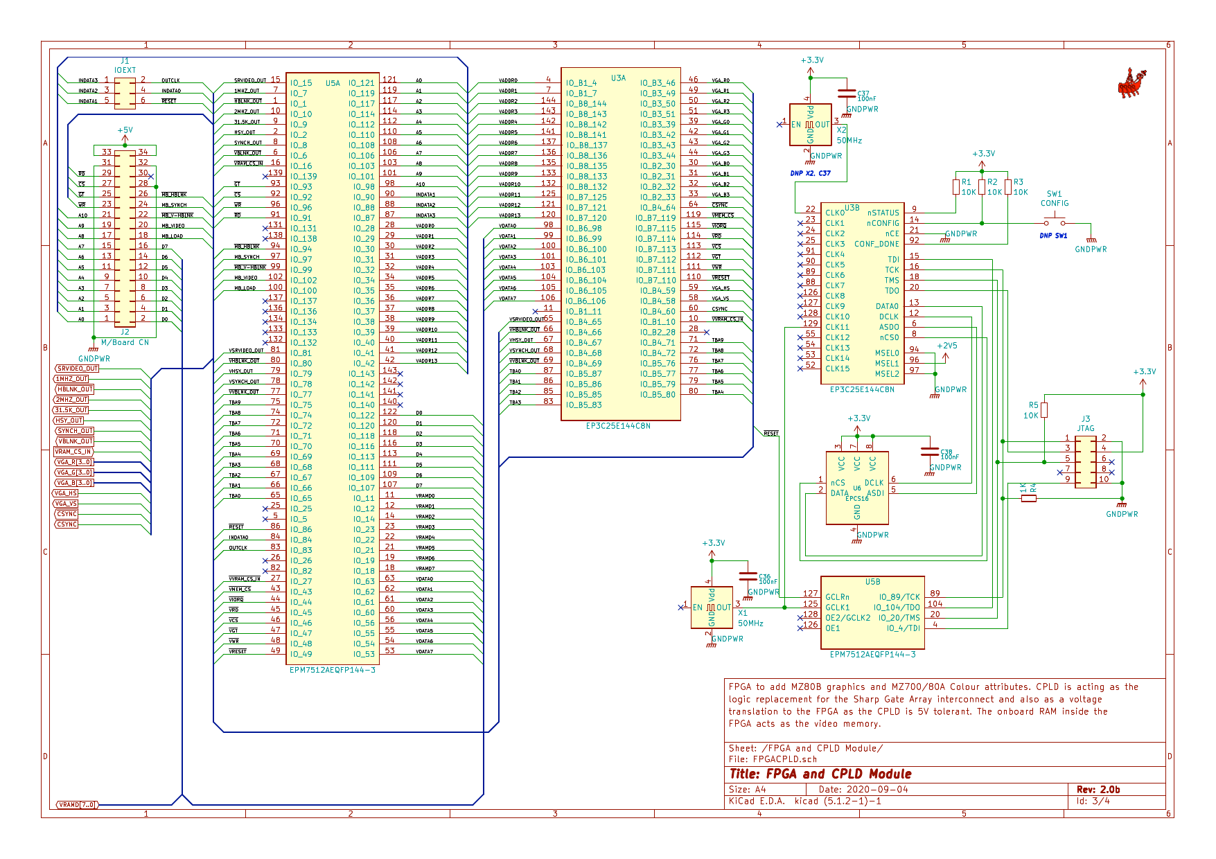
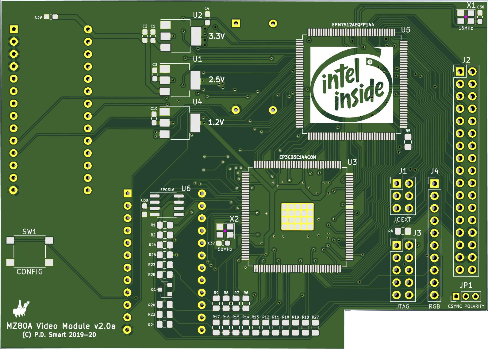
The core of this design is an FPGA to replace all the discrete logic on v1.0. The requirements for v2.0 are to add not only the 40/80 column and Colour capabilities of v1.0 but to add compatibility with the MZ80B and its 2 graphics options and the MZ-700 attributes differences. The video memory is instantiated within the FPGA as BRAM along with all the logic.
The CPLD's primary role is to translate 5V from the Sharp logic into 3.3V of the FPGA, the latter not being 5V tolerant. It also takes on replacing some of the logic found in the MB14298/MB14299 gate arrays such as frequency generation and timing.
v2.0 VGA Output Schematic
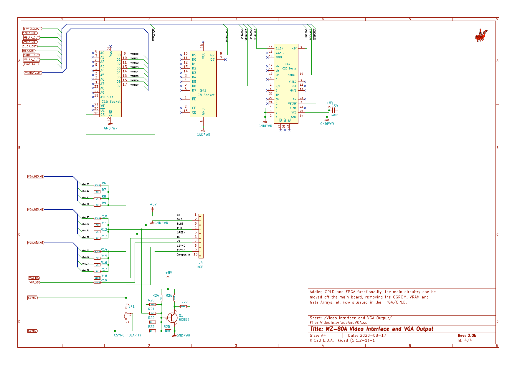
In contrast to version 1.0, version 2.0 doesnt reuse the existing gate arrays, video shift register, CGROM and RAM, these are removed from the mainboard and simple connectivity is made via their sockets. ie. The video is created by the output (pin 9) of the 74LS165 along with the Sync from the MB14298 (HSY and SYNCH), these locations are lifted off the mainboard and fed from the CPLD.
In addition, true 4 bit RGB output is now fed to the RGB and composite outputs. The Sharp is only monochrome on the MZ80B and 8 colour foreground + 8 colour background on the MZ-700/80A but making this small addition increases flexibility in the range of colours for features such as the MZ80A colour intensity signal and future expansion.
v2.0 Power Supply Schematic
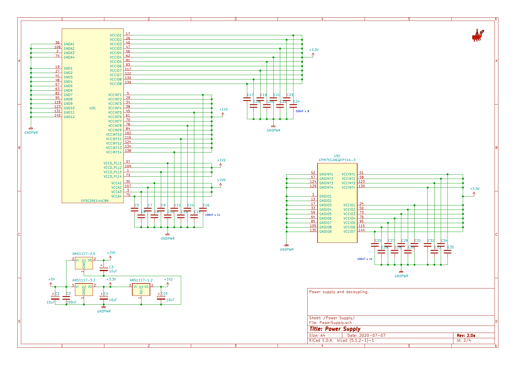
Using FPGA's in a design bring about more complex power requirments. The Sharp MZ80A uses 3 voltages, 12V, 5V and -5V and the FPGA adds 3.3V, 2.5V and 1.2V! Luckily everything on this design is based on 5V taken from an uplifted socket and the CN1 connector from the mainboard, so just adding standard LDO regulators to create the 3 additional voltages along with sufficient decoupling as specified by Altera is all that is required.
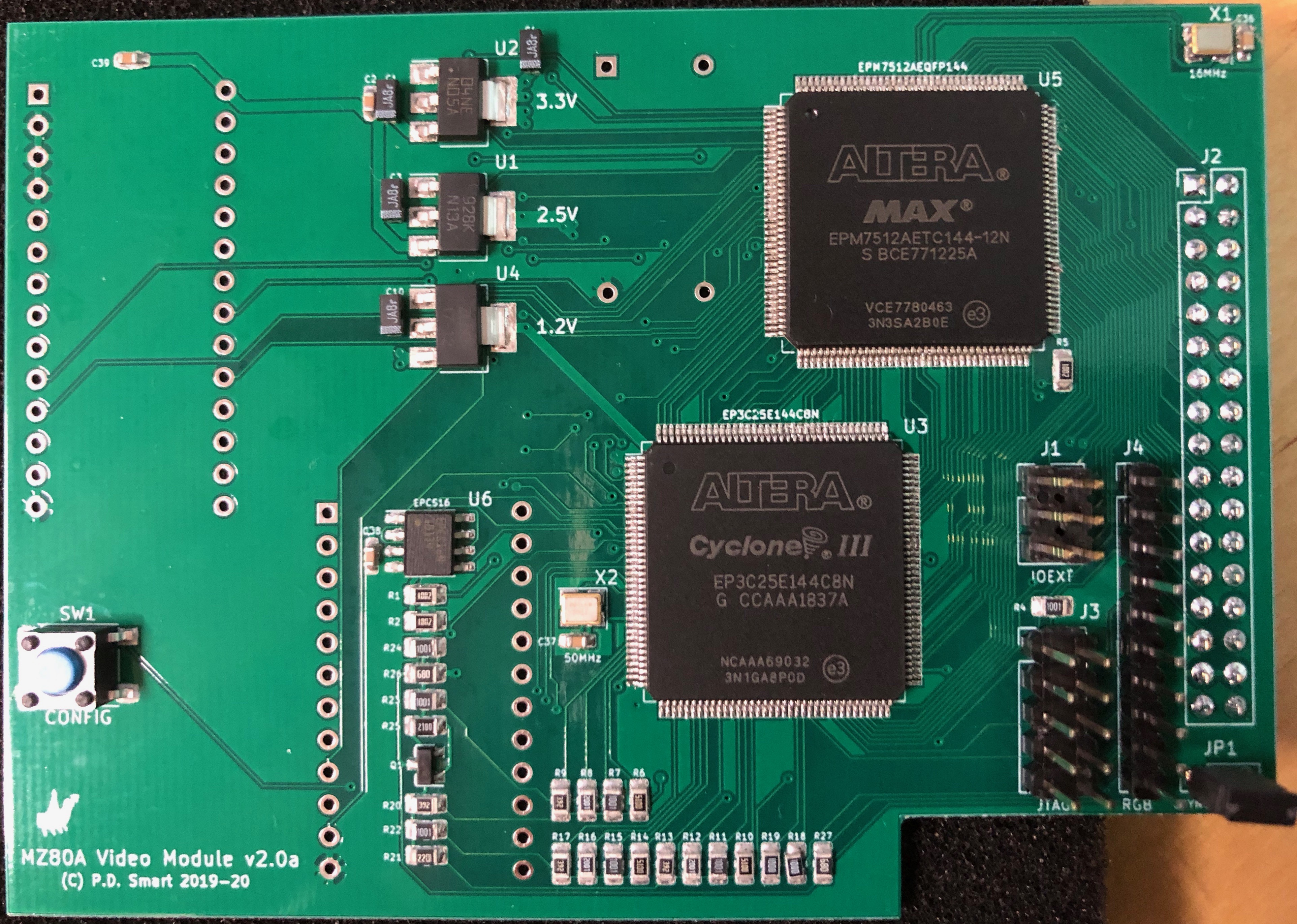
v2.0 PCB
v2.0 Installation Notes
In order to upgrade the video on a Sharp MZ-80A you need to be able to inject new video control signals into the serialiser IC 8 (74LS165), basically the load and clock pulse signals change according to 40/80 mode. The only way to do this is to cut tracks or remove the IC. As I dont like modifying vintage equipment I chose the later, ie. remove IC 8 and install a socket. Using this method the machine can be returned to original at any time by reinstalling the 74LS165.
Note, a tranZPUter or tranZPUter SW needs to be installed before making this change, without it the Video Module wont start up.
If you are familiar with electronics and soldering then the modification is straight forward by following the below instructions:
1) Remove the two screws under the keyboard at the front of the machine, one in each corner.
2) Remove the 4 screws on the monitor legs.
3) Unplug the speaker cable which runs up the side of the monitor and onto a two pronged connector. NB. Dont do this if you have just switched off the monitor, wait a while.
4) At the rear of the machine just behind the CRT control signal input on the end of the CRT glass neck, to the left, is a small daughter board which holds the RESET, Volume, Brightness controls. Gently pry this loose from the two restrainers. Dont put too much pressure on the restrainers, the machine is 40 years old so they have probably lost their flexibility.
5) Trace the orange cable from the CRT to the motherboard and unplug (there are two, one is for the CRT, the other for the tape deck).
6) Just below the CRT control board, on the motherboard is a 2 pin connector with a grey wire, the RESET signal (you can trace it back from the daughter board removed in 4. Unplug it.
7) Gently lift out the CRT monitor and place in a safe location.
8) Remove the 3 screws holding the keyboard down and hinge forward.
9) At the rear of the motherboard are two screws, one in each corner, remove them.
10) Unplug the thick black earth wire coming from the PSU.
11) Unplug the PSU connector (Red, Yellow, Black and Blue wires identify it).
12) Unplug the tape deck orange cable.
13) Gently disconnect the keyboard ribbon cable, grab each side and gently pull in a rocking motion to release it from the push fit connector.
14) Gently raise and remove the motherboard, it will need a bit of back pressure. Dont try to bend the 3 plastic clips at the front of the motherboard, the plastic after 40 years is no longer as flexible as it once was!
15) Locate IC8 on the rear left side of the board, the two 28 pin Sharp branded Gate Arrays are a good locator.
16) Turn the board upside down and desolder the IC.
17) Install a 16 pin socket in the location of IC8.
18) Re-install the motherboard, again take care with the plastic clips, restore the two screws which hold it down.
19) Reconnect the black ground wire from the PSU.
20) Reconnect the PSU cable, the Red lead goes to the rear of the machine, blue faces to the front of the machine,
21) Reconnect the tape deck cable, it goes into the front most of the two similar connectors. The cable has one pin missing, that side of the connector should face to the right, looking at the motherboard from front to rear.
22) Reconnect the keyboard ribbon cable. Line it up holding both sides and gently but firmly push it into the connector, ie. the long black connector just in front of Resistor Array RA2.
23) Remove the IC's 20 and 31 from their sockets. These are the Sharp Gate arrays which provide glue logic for the video and Z80 control.
24) Remove the video RAM IC 15 from its socket.
25) Take the Video Module v2.0 and install it, lining up the underside socket raisers (3 off) with it's corresponding socket. Be careful here as it is easy to bend the raiser pins and they dont take much to snap. I use the end connector CN2 as the point of reference, once lined up on CN2, gently push the board down. If you feel any resistence then check underneath, best with a smart phone camera, to ensure the raiser pins are lining up with their relevant socket.
26) Connect the 6pin ribbon cable between J1/IOEXT on the Video Module and J2/Video Ext on the tranZPUter SW board.
27) Bring the CRT monitor close to the machine and reconnect the orange cable.
28) Power on and verify all is working, ie. video is displayed and keyboard works etc.
29) Turn off and wait several minutes, or be very careful, the CRT still has high voltage within it's capacitors, reinstall the monitor. The monitor should line up on the main house base and click into place. The orange cable should already be connected from 27 above.
30) Reconnect the 2 pin RESET connector, the one with the grey wire, it goes onto the motherboard just below the CRT main board, approx in the middle.
31) Reinstall the rear daughter board, the one housing the Reset, Volume and Brightness controls. Do this by lining it up with the cutouts and gently push, it will click into place.
32) Reinstall the 4 screws holding the monitor to the main housing and tighten.
33) Reconnect the 2 pin speaker wire onto the CRT mainboard. It is very difficult to see the connector as it is just 2 protruding pins. The speaker wire then runs down the side of the monitor in the grooves provided.
34) Put the keyboard down flat and re-insert the 3 screws holding it down.
35) Power check to verify if all is still working, if it isnt, verify from step 26 maybe something has been skipped.
36) Close the lid and reinsert the two screws at the front of the unit below the keyboard to fasten the lid down.
If you are not comfortable with electronics then the best option is to find a friend or local repair shop who can make the change.
Design Detail
Video Module v2.x
Using the FPGA allows the Video Module v2.x to provide video capabilites for nearly all the Sharp MZ series, ie: MZ-80K, MZ-80C, MZ-1200, MZ-80A, MZ-700, MZ-80B (including graphics). In the near future the video capabilities will be upgraded to include the MZ-800 and MZ-2000 machines. To use a specific machines video capabilities, a mode (described below) is written into the mode register to select the required video capabilites based on machine model and you then use the normal methods of accessing the video of the selected machine ie. 0xD000-0xD7FF for video on an MZ-80A. This includes functions such as the invert or hardware scroll functionality.
An addition to the original Sharp MZ series capabilites, is the addition of a 640x200/320x200 8 colour Graphics frame buffer. This frame buffer is made up of 3x16K RAM blocks, 1 per colour with a resolution of 640x200 which matches the output display buffer bit for bit. If the display is working at 40x25 characters then the resolution is 320x200, otherwise for 80x25 it is 640x200.
For all modes except 640x200 the display is double buffered whereby the image is assembled in a seperate buffer to the one which is rendered for screen display. Due to lack of memory in the Cyclone III FPGA, in 640x200 mode the display isnt double buffered and therefore an optional WAIT state generator can be enabled to prevent screen snow/tear as required.
The RAM for the Graphics frame buffer can be switched into the main CPU address range C000H – FFFFH by programmable registers, 1 bank at a time (ie. Red, Green, Blue banks). This allows for direct CPU addressable pixels to be read and/or written. Each pixel is stored in groups of 8 (1 byte in RAM) scanning from right to left per byte, left to right per row, top to bottom. Ie. if the Red bank is mapped into CPU address space, the byte at C000H represents red pixels 7 - 0 of 320/640 (X) at pixel 0 of 200 (Y). Thus 01H written to C000H would set Pixel 7 (X), Row 0 (Y) to On, 80H written to C000H would set pixel 0 (X), Row 0 (Y) . This applies for Green and Blue banks when mapped into CPU address space.
In order to speed up the display, there is a Colour Write register (similar to what is available on the Sharp MZ-2500), so that a write to the graphics RAM will update all 3 banks at the same time which allows for immediate colour write.
Programmable Registers
In order to make use of the video functionality a set of registers have been designed through which all functions can be accessed.
The functionality is grouped as follows:
- Control - set the video capability mode, set the column width, set the colour/mono capabilities.
- Graphics - configure the graphics capability.
- GPU - offload tasks to the inbuilt graphics processor to speed up video tasks.
- Palette - set and configure the display palette.
The registers lie in the upper I/O region from 0xD0 - 0XFD and are accessed with standard Z80 I/O commands IN/OUT. Unless otherwise stated, all registers are read/write and a read will return the current value stored.
Control Register (0xF8 - 248 decimal)
This is the video mode register. It specifies the hardware model the Video Module should function as in addition the column width and colour abilities of the output display.
| Bits | Dir | Description |
|---|---|---|
| 2:0 | R/W | Set the hardware model of the Video Module. 000 = MZ-80K 001 = MZ-80C 010 = MZ-1200 011 = MZ-80A 100 = MZ-700 101 = MZ-800 110 = MZ-80B 111 = MZ-2000 |
| 3 | R/W | Set the column width of the video output. 0 = 40 Column, 1 = 80 Column |
| 4 | R/W | Set the colour capabilities of the video output. 0 = Monochrome, 1 = Colour. |
| 5 | R/W | Enable the Programmable Character Generator RAM. 0 = disabled, 1 = enabled. |
| 7:6 | R/W | Set the VGA mode. 00 = Original MZ video format, 15.62KHz Horizontal x 60Hz Vertical. 01 = VGA 640x480 @ 60Hz 10 = VGA 1024x768 @ 60Hz 11 = VGA 800x600 @ 60Hz. |
Graphics Mode Register (0xF9 - 249 decimal)
This is the graphics mode control register. It specifies what video is to be output, how it is blended and which Graphics RAM bank can be read/written to.
| Bits | Dir | Description |
|---|---|---|
| 1:0 | R/W | Read mode (00=Red Bank, 01=Green Bank, 10=Blue Bank, 11=Not used). Select which bank to be read when enabled in CPU address space. |
| 3:2 | R/W | Write mode (00=Red Bank, 01=Green Bank, 10=Blue Bank, 11=Indirect). Select which bank to be written to when enabled in CPU address space. |
| 4 | R/W | VRAM Output. 0=Enable, 1=Disable. Output Character RAM to the display. |
| 5 | R/W | GRAM Output. 0=Enable, 1=Disable. Output Graphics RAM to the display. |
| 7:6 | R/W | Blend Operator (00=OR ,01=AND, 10=NAND, 11=XOR). Operator to blend Character display with Graphics Display. |
Colour Writer Registers (0xFA - 250 decimal to 0xFC - 252 decimal)
For Indirect mode (Control Register bits 3/2 set to 11), a write to the Graphics RAM when mapped into CPU address space C000H – FFFFH will see the byte masked by the Red Colour Writer Register and written to the Red Bank with the same operation for Green and Blue. This allows rapid setting of a colour across the 3 banks.
ie. Red Filter = 0x80, Green Filter = 0x40, Blue Filter = 0x20, then an indirect write to address C000H will set pixel 0,0 to red, 1,0 to green, 2,0 to blue.
| Bit | Dir | Pixel | I/O Addr | Colour | Description |
|---|---|---|---|---|---|
| 0 | R/W | 7 | 0xFAH | Red | Set to Red during indirect write. |
| 1 | R/W | 6 | 0xFAH | Red | |
| 2 | R/W | 5 | 0xFAH | Red | |
| 3 | R/W | 4 | 0xFAH | Red | |
| 4 | R/W | 3 | 0xFAH | Red | |
| 5 | R/W | 2 | 0xFAH | Red | |
| 6 | R/W | 1 | 0xFAH | Red | |
| 7 | R/W | 0 | 0xFAH | Red | Set to Red during indirect write. |
| 0 | R/W | 7 | 0xFBH | Green | Set to Green during indirect write. |
| 1 | R/W | 6 | 0xFBH | Green | |
| 2 | R/W | 5 | 0xFBH | Green | |
| 3 | R/W | 4 | 0xFBH | Green | |
| 4 | R/W | 3 | 0xFBH | Green | |
| 5 | R/W | 2 | 0xFBH | Green | |
| 6 | R/W | 1 | 0xFBH | Green | |
| 7 | R/W | 0 | 0xFBH | Green | Set to Green during indirect write. |
| 0 | R/W | 7 | 0xFCH | Blue | Set to Blue during indirect write. |
| 1 | R/W | 6 | 0xFCH | Blue | |
| 2 | R/W | 5 | 0xFCH | Blue | |
| 3 | R/W | 4 | 0xFCH | Blue | |
| 4 | R/W | 3 | 0xFCH | Blue | |
| 5 | R/W | 2 | 0xFCH | Blue | |
| 6 | R/W | 1 | 0xFCH | Blue | |
| 7 | R/W | 0 | 0xFCH | Blue | Set to Blue during indirect write. |
Memory Page Registers (0xFD - 253 decimal)
This register is responsible for enabling Video memory into Z80 address space. It is possible to enable 1 of the 3 colour 16KB GRAM (chosen via the Graphics Mode register) into Z80 address C000:FFFF or the CGROM into Z80 address space D000:DFFF. This register overrides all other memory page settings.
| Bits | Dir | Description |
|---|---|---|
| 0 | R/W | Switches in a 16Kb graphics ram bank to C000 - FFFF. The bank (or colour) is selected by the Graphics Mode register. 0 = Off, normal Z80 memory operations. 1 = 16KB GRAM enabled. Setting this register overrides all MZ-700/MZ-80B specific memory page settings. |
| 7 | R/W | Switches in CGROM for upload at D000:DFFF. 0 - Normal memory operations, 1 - CGROM paged in. |
Video Module Status Register (0xFD - 253 decimal)
This register reports on the Video Module status. Bits 7 & 0 are reserved for reporting the Memory Page register settings.
| Bits | Dir | Description |
|---|---|---|
| 5 | R | Framebuffer Horizontal Blanking. 1 = Horizontal Blanking active, 0 = no horizontal blanking. |
| 6 | R | Framebuffer Vertical Blanking. 1 = Vertical Blanking active, 0 = no vertical blanking. |
GPU Parameters Register (0xF6 - 246 decimal)
A read from this register pops off bits 7:0 then shifts the register right by 8 bits.
GPU Command Register (0xF7 - 247 decimal)
| Command | Parameters | Description |
|---|---|---|
| 0x00 | n/a | No operation. This is the idle state command when the GPU isnt busy, issuing it performs no action. |
| 0x01 | n/a | Clear VRAM screen. The entire video and attribute RAM are cleared to space character (ie. blank) with white characters on a blue background. |
| 0x02 | [15:8] - character [7:0] - attribute byte |
Clear VRAM screen with char and attribute. The entire video and attribute RAM are cleared to the values given in the parameter list. |
| 0x03 | [47:40] - Start X [39:32] - Start Y [31:24] - End X [23:16] - End Y [15:8] - display char [7:0] - attribute byte. |
A portion of the video and attribute RAM are cleared to the given character and attribute value, starting at Start X/Y and finishing at End X/Y. |
| 0x81 | n/a | The entire 16KB frambuffer (red/green/blue) is cleared. |
| 0x82 | [87:72] - Start X [71:56] - Start Y [55:40] - End X [39:24] - End Y [23:16] - Red Filter [15:8] - Green Filter [7:0] - Blue Filter R/G/B Filters are 8 pixel wide, bit 7 is the leftmost pixel. |
A section of the 16KB frambuffer (red/green/blue) is cleared according to the given parameters. Cleared area is from Start X/Y to End X/Y and the filters set the pixels in this area according to their values. 1 = set the corresponding pixel, 0 - clear the corresponding pixel. |
| 0xFF | n/a | Reset the GPU. Cancel any running operation and return to idle state immediately. |
GPU Status Register (0xF7 - 247 decimal)
This register returns the current GPU status and should be polled before each new command is requested.
| Bits | Dir | Function | Description |
|---|---|---|---|
| 0 | R | BUSY | Flag to indicate busy status of the GPU. 1 = Busy, 0 = Idle. If busy no further command will be processed until the GPU returns to Idle except the RESET command which will be acted on immediately. |
VGA Border Area Register (0xF3 - 243 decimal)
In VGA modes, the expansion of the graphics RAM/VRAM doesnt quite fill the entire display area which is normally left blank. This register allows attributes to be set so that different colours can be applied as needed.
| Bits | Dir | Description |
|---|---|---|
| 2:0 | R/W | Set the border colour. 2: = Red 1: = Green 0: = Blue |
Select Palette Register (0xF5 - 245 decimal)
There are 256 palettes, 0 is the default with system colours, 1..255 are fixed palettes at time of FPGA HDL compilation. The palettes can be reprogrammed via the palette configuration registers described below.
Select Palette Configration Off Pointer Register (0xD3 - 211 decimal)
This register sets the palette number to be configured when a pixel (R/G/B) is in the off state. ie. colour to be output when the pixels are off. A write to this register is made prior to writing into the actual palette colour registers.
Select Palette Configration On Pointer Register (0xD4 - 212 decimal)
This register sets the palette number to be configured when a pixel (R/G/B) is in the on state. ie. colour to be output when the pixels are on. A write to this register is made prior to writing into the actual palette colour registers.
Set Palette Red Value Register (0xD5 - 213 decimal)
This register sets the 5 bit Red value to be used in the palette selected via The Off/On Pointer Registers.
Set Palette Green Value Register (0xD6 - 214 decimal)
This register sets the 5 bit Green value to be used in the palette selected via The Off/On Pointer Registers.
Set Palette Blue Value Register (0xD6 - 214 decimal)
This register sets the 5 bit Blue value to be used in the palette selected via The Off/On Pointer Registers.
Set Video Mode Parameter Register (0xD0 - 208 decimal)
The table below outlines the current video modes and parameter numbers. The active mode is set by the Control Register and the parameters can then be updated via the Video Mode parameter registers.
Front porch is included in the XXX_SYNC_START parameters. Back porch is included in the XXX_LINE_END, ie. XXX_LINE_END - XXX_SYNC_END = Back Porch.
| Param Number | 0 | 1 | 2 | 3 | 4 | 5 | 6 | 7 | 8 | 9 | 10 | 11 | 12 | 13 | 14 | 15 | 16 | 17 | 18 | |
|---|---|---|---|---|---|---|---|---|---|---|---|---|---|---|---|---|---|---|---|---|
| Mode | Description | H_DSP_START | H_DSP_END | H_DSP_WND_START | H_DSP_WND_END | V_DSP_START | V_DSP_END | V_DSP_WND_START | V_DSP_WND_END | H_LINE_END | V_LINE_END | MAX_COLUMNS | H_SYNC_START | H_SYNC_END | V_SYNC_START | V_SYNC_END | H_POLARITY | V_POLARITY | H_PX | V_PX |
| 0 | MZ80K/C/1200/A machines have a monochrome 60Hz display with scan of 512 x 260 for a 320x200 viewable area. | 0 | 320 | 0 | 320 | 0 | 200 | 0 | 200 | 511 | 259 | 40 | 320 + 43 | 320 + 43 + 45 | 200 + 19 | 200 + 19 + 4 | 0 | 0 | 0 | 0 |
| 1 | MZ80K/C/1200/A machines with an adapted monochrome 60Hz display with scan of 1024 x 260 for a 640x200 viewable area. | 0 | 640 | 0 | 640 | 0 | 200 | 0 | 200 | 1023 | 259 | 80 | 640 + 106 | 640 + 106 + 90 | 200 + 19 | 200 + 19 + 4 | 0 | 0 | 0 | 0 |
| 2 | MZ80K/C/1200/A machines with MZ700 style colour @ 60Hz display with scan of 512 x 260 for a 320x200 viewable area. | 0 | 320 | 0 | 320 | 0 | 200 | 0 | 200 | 511 | 259 | 40 | 320 + 43 | 320 + 43 + 45 | 200 + 19 | 200 + 19 + 4 | 0 | 0 | 0 | 0 |
| 3 | MZ80K/C/1200/A machines with MZ700 style colour @ 60Hz display with scan of 1024 x 260 for a 640x200 viewable area. | 0 | 640 | 0 | 640 | 0 | 200 | 0 | 200 | 1023 | 259 | 80 | 640 + 106 | 640 + 106 + 90 | 200 + 19 | 200 + 19 + 4 | 0 | 0 | 0 | 0 |
| 4 | Mode 0 upscaled as 640x480 @ 60Hz timings for 40Char mode monochrome. | 0 | 640 | 0 | 640 | 0 | 480 | 0 | 400 | 799 | 524 | 40 | 640 + 16 | 640 + 16 + 96 | 480 + 10 | 480 + 10 + 2 | 0 | 0 | 1 | 1 |
| 5 | Mode 1 upscaled as 640x480 @ 60Hz timings for 80Char mode monochrome. | 0 | 640 | 0 | 640 | 0 | 480 | 0 | 400 | 799 | 524 | 80 | 640 + 16 | 640 + 16 + 96 | 480 + 10 | 480 + 10 + 2 | 0 | 0 | 0 | 1 |
| 6 | Mode 2 upscaled as 640x480 @ 60Hz timings for 40Char mode colour. | 0 | 640 | 0 | 640 | 0 | 480 | 0 | 400 | 799 | 524 | 40 | 640 + 16 | 640 + 16 + 96 | 480 + 10 | 480 + 10 + 2 | 0 | 0 | 1 | 1 |
| 7 | Mode 3 upscaled as 640x480 @ 60Hz timings for 80Char mode colour. | 0 | 640 | 0 | 640 | 0 | 480 | 0 | 400 | 799 | 524 | 80 | 640 + 16 | 640 + 16 + 96 | 480 + 10 | 480 + 10 + 2 | 0 | 0 | 0 | 1 |
| 8 | Mode 0 upscaled as 1024x768 @ 60Hz timings for 40Char mode monochrome. | 0 | 1024 | 0 | 960 | 0 | 768 | 0 | 600 | 1343 | 805 | 40 | 1024 + 24 | 1024 + 24 + 136 | 768 + 3 | 768 + 3 + 6 | 0 | 0 | 2 | 2 |
| 9 | Mode 1 upscaled as 1024x768 @ 60Hz timings for 80Char mode monochrome. | 0 | 1024 | 0 | 640 | 0 | 768 | 0 | 600 | 1343 | 805 | 80 | 1024 + 24 | 1024 + 24 + 136 | 768 + 3 | 768 + 3 + 6 | 0 | 0 | 0 | 2 |
| 10 | Mode 2 upscaled as 1024x768 @ 60Hz timings for 40Char mode colour. | 0 | 1024 | 0 | 960 | 0 | 768 | 0 | 600 | 1343 | 805 | 40 | 1024 + 24 | 1024 + 24 + 136 | 768 + 3 | 768 + 3 + 6 | 0 | 0 | 2 | 2 |
| 11 | Mode 3 upscaled as 1024x768 @ 60Hz timings for 80Char mode colour. | 0 | 1024 | 0 | 640 | 0 | 768 | 0 | 600 | 1343 | 805 | 80 | 1024 + 24 | 1024 + 24 + 136 | 768 + 3 | 768 + 3 + 6 | 0 | 0 | 0 | 2 |
| 12 | Mode 0 upscaled as 800x600 @ 60Hz timings for 40Char mode monochrome. | 0 | 800 | 0 | 640 | 0 | 600 | 0 | 600 | 1055 | 627 | 40 | 800 + 40 | 800 + 40 + 128 | 600 + 1 | 600 + 1 + 4 | 1 | 1 | 1 | 2 |
| 13 | Mode 1 upscaled as 800x600 @ 60Hz timings for 80Char mode monochrome. | 0 | 800 | 0 | 640 | 0 | 600 | 0 | 600 | 1055 | 627 | 80 | 800 + 40 | 800 + 40 + 128 | 600 + 1 | 600 + 1 + 4 | 1 | 1 | 0 | 2 |
| 14 | Mode 2 upscaled as 800x600 @ 60Hz timings for 40Char mode colour. | 0 | 800 | 0 | 640 | 0 | 600 | 0 | 600 | 1055 | 627 | 40 | 800 + 40 | 800 + 40 + 128 | 600 + 1 | 600 + 1 + 4 | 1 | 1 | 1 | 2 |
| 15 | Mode 3 upscaled as 800x600 @ 60Hz timings for 80Char mode colour. | 0 | 800 | 0 | 640 | 0 | 600 | 0 | 600 | 1055 | 627 | 80 | 800 + 40 | 800 + 40 + 128 | 600 + 1 | 600 + 1 + 4 | 1 | 1 | 0 | 2 |
H_DSP_START = Horizontal display area start. ie. the physical display area for given mode.
H_DSP_END = Horizontal display area end.
H_DSP_WND_START = Horizontal display window start. ie. the actual display area when data is output.
H_DSP_WND_END = Horizontal display window end.
V_DSP_START = Vertical display area start.
V_DSP_END = Vertical display area end.
V_DSP_WND_START = Vertical display area window start.
V_DSP_WND_END = Vertical display area window start.
H_LINE_END = Horizontal line end, ie. last horizontal pixel.
V_LINE_END = Vertical line end, last vertical pixel.
MAX_COLUMNS = Maximum character display columns.
H_SYNC_START = Horizontal sync start.
H_SYNC_END = Horizontal sync end.
V_SYNC_START = Vertical sync start.
V_SYNC_END = Vertical sync end.
H_POLARITY = Horizontal sync polarity, 0 = negative, 1 = positive.
V_POLARITY = Vertical sync polarity, 0 = negative, 1 = positive.
H_PX = Horizontal pixel doubling, ie. 1x, 2x, 4x etc.
V_PX = Vertical pixel doubling, ie. 1x, 2x, 4x etc.
Set Video Mode Lower Parameter Byte Register (0xD1 - 209 decimal)
This register is used to write the lower byte of the parameter selected with the Video Mode Parameter Register. ie. If Parameter 0 is set, then a write to this register will update the lower byte of the H_DSP_START parameter.
Set Video Mode Upper Parameter Byte Register (0xD2 - 210 decimal)
This register is used to write the upper byte of the parameter selected with the Video Mode Parameter Register. ie. If Parameter 0 is set, then a write to this register will update the upper byte of the H_DSP_START parameter.
Software Version 1
All control is performed through the latch IC U9 (v1.0) or U11 (v1.1) at address location 0xDFFF.
This address is shared between the attribute RAM and the control latch. In version 1.0 it was deemed free when I started the project as it should have been off screen but I overlooked the hardware scrolling and so a write to this location *may* corrupt the attribute of the last character and only if it is visible when the Character RAM is scrolled to the bottom.
In version 1.1 this bug has been corrected by a multivibrator circuit which is triggered when a read is made to 0xDFFF and reset in just over one Z80 instruction cycle, thus allowing for a LD HL, 0xDFFF; LD B, 0x80; LD A,(HL); LD (HL), B operation to change the latch state.
The table below shows the bit functions of the IC U9/U11 which is a 74HCT373 octal latch. A switch from 40 to 80 column mode requires a write of 0x80 into the control address 0xDFFF.
| Bit | Function | Description |
|---|---|---|
| 0 | Character ROM Set Bit 0 | Select one of 4 sets of Character Generator ROMS. |
| 1 | Character ROM Set Bit 1 | |
| 2 | Unused | |
| 3 | Unused | |
| 4 | Unused | |
| 5 | Unused | |
| 6 | Unused | |
| 7 | 40/80 Column Mode | Enable 80 Column mode when set to 1, 40 Column when set to 0 (default) |
The Character Generator ROM on the Colour Board allows for upto 16 CG-ROM images to be stored and selected. On most of the MZ80 machines, the CG-ROM is 2K in size. On the MZ700/800 it is 4K in size. I havent yet obtained all the possible Sharp CG-ROM images so for the time being, the Character Generator Flash RAM IC U10) is loaded as follows:
| Slot | Attribute Bits 7,3 | U9 Latch Bits 0:1 | Size | ROM | Description |
|---|---|---|---|---|---|
| 0 | 0,0 | 0,0 | 2K | mz-80acg.rom | MZ80A European CG-ROM |
| 1 | 0,1 | 0,0 | 2K | MZ80K_cgrom.rom | MZ80K European CG-ROM |
| 2 | 1,0 | 0,0 | 2K | MZ80K2E_Jap_cgrom.rom | MZ80K Japanese CG-ROM |
| 3 | 1,1 | 0,0 | 2K | MZFONT.rom | Unknown origin CG-ROM |
| 4 & 5 | 0,0 - 0,1 | 0,1 | 4K | MZ700_cgrom.rom | MZ700 European CG-ROM (2 banks) |
| 6 & 7 | 1,0 - 1,1 | 0,1 | 4K | MZ700_cgrom_jp.rom | MZ700 Japanese CG-ROM (2 banks) |
| 8 | 0,0 | 1,0 | 2K | mz-80acg.rom | MZ80A European CG-ROM |
| 9 | 0,1 | 1,0 | 2K | MZ80B.rom | MZ80B European CG-ROM |
| 10 | 1,0 | 1,0 | 2K | mz-80acg.rom | MZ80A European CG-ROM |
| 11 | 1,1 | 1,0 | 2K | mz-80acg.rom | MZ80A European CG-ROM |
| 12 | 0,0 | 1,1 | 2K | mz-80acg.rom | MZ80A European CG-ROM |
| 13 | 0,1 | 1,1 | 2K | mz-80acg.rom | MZ80A European CG-ROM |
| 14 | 1,0 | 1,1 | 2K | mz-80acg.rom | MZ80A European CG-ROM |
| 15 | 1,1 | 1,1 | 2K | mz-80acg.rom | MZ80A European CG-ROM |
This image is created by the shell script in the repository, [ABS PATH]/software/tools/make_cgrom.sh and can be executed as follows:
cd [ABS PATH]/software
./tools/make_cgrom.sh
The output image, ie. ../../MZ80A_80COLOUR/software/roms/COLOURBOARD_CG.rom, can be directly flashed into a 28C256 Flash RAM and mounted on the Colour Board.
In order to set a colour on the colour output, an attribute byte is written into the attribute RAM for each character written to the Character RAM. The bits of the attribute RAM have the following function:
| Bit | Function |
|---|---|
| 0 | Background Blue |
| 1 | Background Red |
| 2 | Background Green |
| 3 | Character ROM Bit 0 |
| 4 | Foreground Blue |
| 5 | Foreground Red |
| 6 | Foreground Green |
| 7 | Character ROM Bit 1 |
To write a Blue character on a Black background for a character 'A' at screen position 0,0 - write 0x41 to Character RAM location 0xD000, write 0x10 to attribute RAM location 0xD800. This assumes Character Generator subset 0.
To select one of the 4 Character Generator Sets, bits 1:0 are set in IC U9/U11. Then to select one of 4 character subsets, you set the attribute bits 7 & 3 as per the table above.
ie. If you set bits 1:0 to '00' in UC U9/U11, you will activate character generator set 0 in slots 0-3. If you then write 0x41 into location 0xD000, 0x42 into 0xD001, 0x14 into location 0xD800 and 0xF0 into 0xD801 you will see onscreen the letter A in blue on black background and a Japanese character in white on black background just after it.
Software Version 2
- VideoInterface - This is the CPLD and it directly interfaces with the original Sharp MZ80A mainboard hardware being 5V tolerant. It acts as a gateway between the mainboard and the FPGA and provides signals to the mainboard which would have originally been provided by the MB14298/MB14299 gate arrays.
- VideoController - This is the FPGA and it provides all of the video functionality including RAM.
The VideoController provides all the Video capabilities including pixel mapped graphics and Sharp MZ series video functionality.
Repository Structure
Paths
For ease of reading, the following shortnames refer to the corresponding path in this chapter.
| Short Name | Path | Description |
|---|---|---|
| [<ABS PATH>] | The path where this repository was extracted on your system. | |
| <80COL> | [<ABS PATH>]/MZ80A_80COLOUR/ | Repository root directory. |
| <CPLD> | [<ABS PATH>]/MZ80A_80COLOUR/CPLD | Complex Programmable Logic Device RTL and build files used for the VideoInterface. |
| <FPGA> | [<ABS PATH>]/MZ80A_80COLOUR/FPGA | Field Programmable Gate Array RTL and build files used for the VideoController. |
| <PCB> | [<ABS PATH>]/MZ80A_80COLOUR/pcb | Gerber files for creating a PCB, each version in seperate sub-directory. |
| <SCHEMATICS> | [<ABS PATH>]/MZ80A_80COLOUR/schematics | Kicad schematics and PCB design files including component library definitions. |
| <SOFTWARE> | [<ABS PATH>]/MZ80A_80COLOUR/software | Root directory for software used in the project. |
| <TOOLS> | [<ABS PATH>]/MZ80A_80COLOUR/software/tools | Shell scripts to make the Character Generator ROM. |
| <ROMS> | [<ABS PATH>]/MZ80A_80COLOUR/software/roms | Original character generator ROMS and the combined ROM for the project. |
| <MIF> | [<ABS PATH>]/MZ80A_80COLOUR/software/mif | Memory Initialisation Files for the FPGA. Contains CG ROMS and Palette ROMS |
| <DOCKER> | [<ABS PATH>]/MZ80A_80COLOUR/docker | Docker description files to build a docker image to run Altera Quartus Prime. |
| <DOCS> | [<ABS PATH>]/MZ80A_80COLOUR/docs | Any documentation relevant to the project. |
RTL
| Folder | RTL File | Description |
|---|---|---|
| <CPLD> | VideoInterface_pkg.vhd | The Video Interface configuratioon file. |
| VideoInterface_TopLevel.vhd | The top level design file which joins the pin definitions to the actual Video Interface module. | |
| VideoInterface.vhd | The main module describing the required logic for the video interface. | |
| <CPLD>/build | VideoInterface.qpf | The Altera project definition file, the entry point in Quartus II for this project. |
| VideoInterface.qsf | The Altera project resource file which desribes the hardware to be used, the settings and the assignment of CPLD pins to be used in the project. | |
| VideoInterface_constraints.sdc | The timing contraints file to setup timing definitions and restrictions which guide the compiler during compilation of the project. | |
| <FPGA> | VideoController_pkg.vhd | The Video Controller configuratioon file. |
| VideoController_TopLevel.vhd | The top level design file which joins the pin definitions to the actual Video Controller module. | |
| VideoController.vhd | The main module describing the required logic for the video controller. | |
| <CPLD>/build | VideoController.qpf | The Altera project definition file, the entry point in Quartus II for this project. |
| VideoController.qsf | The Altera project resource file which desribes the hardware to be used, the settings and the assignment of FPGA pins to be used in the project. | |
| VideoController_constraints.sdc | The timing contraints file to setup timing definitions and restrictions which guide the compiler during compilation of the project. | |
| Clock_* | Refactored Altera PLL definitions for various development board source clocks. These need to be made more generic for eventual inclusion of Xilinx fabric. | |
| <FPGA>/devices | RAM | Dual Port RAM |
Hardware Description Language
There are various means of creating a bitmap but generally a Hardware Descripion Language is used which resembles software source code. I chose to use VHDL as this was based on ADA, a language I learnt at university. I have used Verilog and System Verilog and find these languages also to be excellent and indeed are used in my Sharp MZ Emulator, but for this project, VHDL is the HDL of choice.
The CPLD and FPGA were both chosen based on easy re-use of the Sharp MZ Emulator code, which used an Intel/Altera Cyclone V, so it made sense to stay with their products. The CPLD, a 512 Macro cell MAX 7000A device, was chosen due to its 5V tolerant capabilities which are not found in more recent devices and would thus require additional voltage translation circuitry to read Sharp MZ-80A signals. The FPGA was chosen on a price/packaging/capabilities requirement, where the device wasnt to be BGA and could incorporate the existing Sharp MZ Emulator video logic HDL, thus requiring at least 64K internal Block RAM. I settled on a Cyclone III EP3C25 device which doesnt quite have enough memory to use all the Sharp MZ Emulator code but after some rework is completely acceptable.
Complex Logic Device - MAX 7000A
The CPLD, term the VideoInterface, is a bridge between the 5V world of the Z80 and the 3.3/2.5/1.2V world of the FPGA. It’s purpose is to provide
- Replacement Sharp VLSI Gate Array logic.
- System and Video clocks (8MHz, 4MHz, 3.54MHz, 2MHz, 1MHZ, 31.5KHz).
- A serialiser which allows the tranZPUter to forward realtime, missing signals not present on the Video Module (ie. A15-A11, Video RDn/WRn, IORQn).
- Software controlled mode control registers.
- Voltage translation
The source files which form the CPLD configuration are:
| Module | Description |
|---|---|
| VideoInterface_TopLevel.vhd | The top level design file, akin to the root schematic of a circuit. It lays out the main component signals entering the CPLD and how they are used. |
| VideoInterface_pkg.vhd | This file contains functions, constant declarations and parameters and is used by all compiled VHDL files/modules. |
| VideoInterface.vhd | The main design file, it contains all the logic to form gate and wire interconnects in the target circuit within the CPLD. |
| build/VideoInterface.qpf | The project file used by Quartus Prime to declare the project and all its files. |
| build/VideoInterface.qsf | The definitions and assignments file. It sets all the parameters for compilation, fitting, pins used and their name, their parameters etc. This file is created by Quartus Prime but often it is quicker to change by hand instead of via the Quartus Prime GUI. |
| build/VideoInterface_constraints.sdc | The timing constraints file created and used by the Time Quest Timing Analysed and also used by the compiler and fitter in deciding on locations where components in the CPLD will be placed. |
Building the CPLD bitstream
You can either install Quartus Prime onto your Windows/Linux workstation or you can create a Docker image as I detail below. After a number of installations on various Linux and Windows flavours, using Docker is by far the easiest way to use this complex package.
Compilation:
   1. Start Quartus Prime v13.0.1, either your local installation or a Docker image.
   2. Go to 'File->Open Project' and search for the directory where your repository clone is stored then select the file in <Clone Path>/MZ80A_80COLOUR/CPLD/build/VideoInterface.qpf, this will open the CPLD VideoInterface project.
   3. Select 'Processing->Start' Compilation - you can safely ignore the warning messages.
   4. When completed, a bitstream will have been created with the name: VideoInterface.sof in the <Clone Path>/MZ80A_80COLOUR/CPLD/build/output_files directory.
Programming:
   1. To upload the bitstream into the CPLD, you need an Altera USB Blaster connected via USB port to the 10pin JTAG IDC connector on the Video Module v2.x board.
   2. In Quartus Prime, go to 'Tools->Programmer' which will start a new Programmer window.
   3. In the Programmer window, click on 'Hardware Setup' and choose your USB adapter and then 'Close'
   4. Click on 'Auto Detect' and it should find 3 devices, an EPM7512AET144, an EP3C25E144 and an EPCS16.
   5. Right click on the EPM7512AET144 device, select Add File then choose the sof file located in <Clone Path>/MZ80A_80COLOUR/CPLD/build/output_files/VideoInterface.sof and click Open.
   6. Select 'Program/Configure' and 'Verify' tick boxes against the EPM7512AET144.
   7. Click on 'Start' and the CPLD should be programmed with the compiled bitstream.
Field Programmable Gate Array
The Cyclone III FPGA of the VideoController provides enhanced video capabilities for the Sharp MZ-80A. Using the Sharp MZ Emulator as it's base, it is able to provide nearly all of the Sharp MZ video hardware capabilities along with colour pixel mapped graphics. It also provides the fledgling start of a GPU (Graphics Processing Unit). The FPGA provides:
- Video capabilities of the Sharp MZ machines: MZ-80K, MZ-80C, MZ-1200, MZ-80A, MZ-700, MZ-80B (including GRAM I/II).
- Colour pixel graphics modes, 8 colour 640x200 and 320x200.
- Internal video modes, ie: Original and Pseudo colour (experimental).
- Multiple external video output modes, ie: Original, VGA 640x480@60Hz, VGA 800x600@60Hz, VGA 1024x768@60Hz.
- Simultaneous internal and external display for Original mode, external only for VGA modes.
| Module | Description |
|---|---|
| VideoController_Toplevel.vhd | The top level design file, akin to the root schematic of a circuit. It lays out the main component signals entering the FPGA and how they are used. |
| VideoController_pkg.vhd | This file contains functions, constant declarations and parameters and is used by all compiled VHDL files/modules. |
| VideoController.vhd | The main design file, it contains all the logic to form gate and wire interconnects in the target circuit within the FPGA. |
| build/VideoController.qpf | The project file used by Quartus Prime to declare the project and all its files. |
| build/VideoController.qsf | The definitions and assignments file. It sets all the parameters for compilation, fitting, pins used and their name, their parameters etc. This file is created by Quartus Prime but often it is quicker to change by hand instead of via the Quartus Prime GUI. |
| build/VideoController_constraints.sdc | The timing constraints file created and used by the Time Quest Timing Analysed and also used by the compiler and fitter in deciding on locations where components in the FPGA will be placed. |
| build/SFL.vhd | The Serial Flash Loader declaration. The Serial Flash Loader is an Altera Megacore IP component used to program serial flash devices connected via the dedicated Serial boot pins. The serial flash device is used to load the FPGA bitstream on power cycle. |
| build/SFL_inst.vhd | The instantiation declaration of the Serial Flash Loader IP used to program the EPCS16 device via the FPGA. |
| build/SFL.qip | The IP declaration of the Serial Flash Loader. It is an Altera Megacore library package. |
| build/Video_Clock.vhd | An FPGA on-board PLL declaration to create various Video base clocks. It is an Altera Megacore IP component. |
| build/Video_Clock_inst.vhd | The instantiation declaration of the PLL IP. |
| build/Video_Clock.qip | The IP declaration of the PLL requirements. |
| build/Video_Clock_II.vhd | The second FPGA on-board PLL declaration to create various Video base clocks. It is an Altera Megacore IP component. Multiple clocks are needed for the Video base frequencies which cant be satisfied with one PLL hence the use of a second PLL. |
| build/Video_Clock_II_inst.vhd | The instantiation declaration of the second PLL IP. |
| build/Video_Clock_II.qip | The IP declaration of the second PLL requirements. |
| build/Video_Clock_III.vhd | The third FPGA on-board PLL declaration to create various Video base clocks. It is an Altera Megacore IP component. Multiple clocks are needed for the Video base frequencies which cant be satisfied with one PLL hence the use of a third PLL. |
| build/Video_Clock_III_inst.vhd | The instantiation declaration of the third PLL IP. |
| build/Video_Clock_III.qip | The IP declaration of the third PLL requirements. |
| build/Video_Clock_IV.vhd | The fourth FPGA on-board PLL declaration to create various Video base clocks. It is an Altera Megacore IP component. Multiple clocks are needed for the Video base frequencies which cant be satisfied with one PLL hence the use of a fourth PLL. |
| build/Video_Clock_IV_inst.vhd | The instantiation declaration of the fourth PLL IP. |
| build/Video_Clock_IV.qip | The IP declaration of the fourth PLL requirements. |
Building the FPGA bitstream
You can either install Quartus Prime onto your Windows/Linux workstation or you can create a Docker image as I detail below. After a number of installations on various Linux and Windows flavours, using Docker is by far the easiest way to use this complex package.
Compilation:
   1. Start Quartus Prime v13.1, either your local installation or a Docker image.
   2. Go to 'File->Open Project' and search for the directory where your repository clone is stored then select the file in <Clone Path>/MZ80A_80COLOUR/FPGA/build/VideoController.qpf, this will open the FPGA VideoController project.
   3. Select 'Processing->Start Compilation' - you can safely ignore the warning messages.
   4. When completed, a bitstream will have been created with the name: VideoController.sof in the <Clone Path>/MZ80A_80COLOUR/FPGA/build/output_files directory.
Programming FPGA:
   1. To upload the bitstream into the FPGA, you need an Altera USB Blaster connected via USB port to the 10pin JTAG IDC connector on the Video Module v2.x board.
   2. In Quartus Prime, go to 'Tools->Programmer' which will start a new Programmer window.
   3. In the Programmer window, click on 'Hardware Setup' and choose your USB adapter and then 'Close'
   4. Click on 'Auto Detect' and it should find 3 devices, an EPM7512AET144, an EP3C25E144 and an EPCS16.
   5. Right click on the EP3C25E144 device, select 'Edit->Add File' then choose the sof file located in <Clone Path>/MZ80A_80COLOUR/CPLD/build/output_files/VideoController.sof and click Open.
   6. Select 'Program/Configure' tick box against the EP3C25E144.
   7. Click on 'Start' and the FPGA should be programmed with the compiled bitstream.
   8. The programming of the FPGA is not persistent, when powered off it will lose the bitmap. To make the programming persistent, following the instructions below to program the EPCS16.
Programming EPCS16:
   1. To upload the bitstream into the EPCS16, a non-volative serial Flash RAM which the FPGA reads on power up you will need an Altera USB Blaster connected via USB port to the 10pin JTAG IDC connector on the Video Module v2.x board.
   2. In Quartus Prime, go to 'File->Convert Programming Files' which will start a new 'Convert Programming File' window.
   3. In the Convert Programming File window:
     3a. Click on 'Programming File Type' and select JTAG Indirect Configuration File.
     3b. Click on 'Configuration Device' and select EPCS16.
     3c. Click on 'File Name' and choose <Clone Path>/MZ80A_80COLOUR/CPLD/build/output_files/VideoController.sof.
     3d. Click on 'Flash Loader' then click on 'Add Device' button. Select Cyclone III -> EP3C25, click on OK.
     3e. Click on 'SOF Data', then click on 'Add File' button. Select the output file which will be <Clone Path>/MZ80A_80COLOUR/CPLD/build/output_files/VideoController.jic, click on OK.
     3f. Click on the 'Generate' button, the output JIC file will now be created as <Clone Path>/MZ80A_80COLOUR/CPLD/build/output_files/VideoController.jic
     3g. Click on 'Close' to close the Convert Programming File window.
   4. In Quartus Prime, go to 'Tools->Programmer' which will start a new Programmer window.
   5. In the Programmer window, click on 'Hardware Setup' and choose your USB adapter and then 'Close'
   6. Click on 'Auto Detect' and it should find 3 devices, an EPM7512AET144, an EP3C25E144 and an EPCS16.
   7. Right click on the EP3C25E144 device, select 'Edit->Add File' then choose the sof file located in <Clone Path>/MZ80A_80COLOUR/CPLD/build/output_files/VideoController.sof and click Open.
   8. Right click on the EPCS16 device, select 'Edit->Add File' then choose the jic file located in <Clone Path>/MZ80A_80COLOUR/CPLD/build/output_files/VideoController.jic and click Open.
   9. Select 'Program/Configure' tick box against the EP3C25E144.
  10. Select 'Program/Configure' and 'Verify' tick boxes against the EPCS16.
  11. Click on 'Start' and the FPGA and the EPCS16 non-volatile Flash RAM should be programmed with the compiled bitstream.
  12. The programming of the FPGA is now persistent and will persist across power cycles.
Quartus Prime in Docker
-
Clone the repository:
 cd ~
 git clone https://github.com/pdsmart/zpu.git
 cd zpu/docker/QuartusPrime
Current configuration will build a Lite version of Quartus Prime. If you want to install the Standard version, before building the docker image:Edit: zpu/docker/QuartusPrime/Dockerfile.13.0.1 Uncomment: '#ARG QUARTUS=QuartusSetup-13.0.1.232.run' Comment out: 'ARG QUARTUS=QuartusSetupWeb-13.0.1.232.run'If you have a license file:
 Copy: <your license file> to zpu/docker/QuartusPrime/files/license.dat
 Edit:  zpu/docker/QuartusPrime/run.sh
 Change: MAC_ADDR="02:50:dd:72:03:01" so that is has the MAC Address of your license file.
Build the docker image:
docker build -f Dockerfile.13.0.1 -t quartus-ii-13.0.1 --build-arg user_uid=`id -u` --build-arg user_gid=`id -g` --build-arg user_name=`whoami` .
For Quartus Prime 13.1 replace 13.0.1 with the necessary version. Quartus Prime 13.0.1 supports the older MAX CPLD devices. Quartus Prime 13.1 supports the older Cyclone III devices. -
Setup your X DISPLAY variable to point to your xserver:
 export DISPLAY=<x server ip or hostname>:<screen number or :<screen number>>
 # ie. export DISPLAY=192.168.1.1:0
On your X server machine, issue the command:
xhost + # or xhost <ip of docker host> to maintain security on a non private network. -
Setup your project directory accessible to Quartus.
Edit: zpu/docker/QuartusPrime/run_quartus.sh Change: PROJECT_DIR_HOST=<location on your host you want to access from Quartus Prime> Change: PROJECT_DIR_IMAGE=<location in Quartus Prime running container to where the above host directory is mapped> # ie. PROJECT_DIR_HOST=/srv/quartus PROJECT_DIR_IMAGE=/srv/quartus -
Run the image using the provided bash script ‘run_quartus.sh’. This script
./run_quartus.sh
This will start Quartus Prime and also an interactive bash shell.
On first start it currently asks for your license file, click 'Run the Quartus Prime software' and then OK. If your home directory is not writeable it will ask you this question everytime you start a new container.
The host devices are mapped into the running docker container so that if you connect a USB Blaster it will be seen within the Programmer tool. As part of the installation I install the udev rules for USB-Blaster and USB-Blaster II as well as the Arrow USB-Blaster driver for use with the CYC1000 dev board. -
To stop quartus prime:
 # Either exit the main Quartus Prime GUI window via File->Exit
 # or
 docker stop quartus
Credits
Licenses
The Gnu Public License v3
The source files are distributed in the hope that it will be useful, but WITHOUT ANY WARRANTY; without even the implied warranty of MERCHANTABILITY or FITNESS FOR A PARTICULAR PURPOSE. See the GNU General Public License for more details.
You should have received a copy of the GNU General Public License along with this program. If not, see http://www.gnu.org/licenses/.